My apologies. I've been looking at board wrong. My camera wouldnt focus so you could see but there are 2 markings for transistors. One on green circuit board and one on yellow board underneath. I was going by the green board that transistors are soldered to but it seems the yellow board is correct. I just confirmed that what I thought was Q125 and R135 are not connected. Its Q118 (thats hot) and its connected to R124.
Its Q118 (thats hot) and its connected to R124.
Please measure the voltages across R126, R127, R128 and R129. Check again R124 and R125, just to be sure.
Edit: was this amp been repaired before ?
Last edited:
R126 0 R128 .2 R127 & R129 .1 R124 .63 R125 .61. I replaced R136 when I first got. That seemed to be only problem at time.Please measure the voltages across R126, R127, R128 and R129. Check again R124 and R125, just to be sure.
Edit: was this amp been repaired before ?
just ordered those 4 transistors just in case. They are almost out of inventory at repuptuble distributors in states.R126 0 R128 .2 R127 & R129 .1 R124 .63 R125 .61. I replaced R136 when I first got. That seemed to be only problem at time.

I agree re Q116 suspicion.Looks like Q116/Q118 are not sharing the current equally. Q116 is suspicious or R126 is open. Q116 is not pulling current at all. What is the resolution of your DMM btw ? I'm asking, just in case. 😉
Edit: @BSST, come over here. I can't do it all by myself mate ! 🙂
Probe Q116 directly at the transistors leads. That should reveal open connections vs. failed Q116.
I cant remember resolution. Its a fluke 87IV. Think its a pretty good meter. Bought at pawn shop over 10 years ago and its still going.Looks like Q116/Q118 are not sharing the current equally. Q116 is suspicious or R126 is open. Q116 is not pulling current at all. What is the resolution of your DMM btw ? I'm asking, just in case. 😉
Edit: @BSST, come over here. I can't do it all by myself mate ! 🙂
DIYAUDIO is crashing on my machine. Just testing that message is getting through.I agree re Q116 suspicion.
Probe Q116 directly at the transistors leads. That should reveal open connections vs. failed Q116.
DIYAUDIO is crashing on my machine. Just testing that message is getting through.
Same here.
Its a fluke 87IV.
Ok, it's a decent meter.
Last edited:
R118 .17v, 78v, .7v R117 & 119 .15v, 78,v .7v R116 .04v, 78v and 0v. I am getting some resistance across the resistor Think it was 1.6 ohm but some of that could have been leads.
DIY server a mess 🙁R118 .17v, 78v, .7v R117 & 119 .15v, 78,v .7v R116 .04v, 78v and 0v. I am getting some resistance across the resistor Think it was 1.6 ohm but some of that could have been leads.
Did you mean Q rather than R? R116 0.4v, 78v and 0v. ---> Q116 b=.04V c= 78V e=0v ???
With closer look, Q118 e,c,b = Q118 e= 0.017, c=78, b= 0.7. ??R118 .17v, 78v, .7v
Then Q116 e=0.04, C=78, b=0. Base still not connected.
Before pulling out Q116, do a continuity test (power off of course). Maybe the base lead is not in contact with the PCB or poor solder joint or something. Well, the drivers/output transistors are soldered to a 'power transistor board' (whatever they call it) which is then connected/soldered to the main board via strip connector. What can go wrong !?

Last edited:
I think my suspicion of Q125 should be set aside, perhaps abandoned (post #57), until Q116 connection is resolved.
Q116 base certainly doesn't seem to be connected to Q118 base--- most likely "floating" and should be sorted out as HighTec suggests. I don't know what to make of Q116 emitter = .04V, but assuming Q116 isn't passing current, then wg_ski absolutely nailed the problem way back in post #8!
Q116 base certainly doesn't seem to be connected to Q118 base--- most likely "floating" and should be sorted out as HighTec suggests. I don't know what to make of Q116 emitter = .04V, but assuming Q116 isn't passing current, then wg_ski absolutely nailed the problem way back in post #8!
You mean Q rather than R? R116 0.4v, 78v and 0v. ---> Q116 b=.04V c= 78V e=0v ???
Yes Q not R. Not sure where brain was yesterday
Yes Q not R. Not sure where brain was yesterday
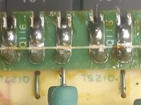
That did it. Thank You a bunch to you guys that stuck with me through this troubleshooting process. It ended up being a ring around a leg of Q116. The solder was still bright and not cold looking like you normally see this problem. The bias /dc offset is still not perfect but should be within range. You cant go below about 10mv dc offset or bias is super low. Ended up setting it at 15mv dc and 40 bias. The only thing I'm a bit concearned about is the 3.2 volt zener has 3.3 volts across it. Will this cause it to burn out soon? Also I took a better picture of the Transistor board with wrong transistor numbers on it that made this troubleshoot process last much longer than it should.Before pulling out Q116, do a continuity test (power off of course). Maybe the base lead is not in contact with the PCB or poor solder joint or something. Well, the drivers/output transistors are soldered to a 'power transistor board' (whatever they call it) which is then connected/soldered to the main board via strip connector. What can go wrong !? View attachment 1119186
Attachments
That was it Thank you.I think my suspicion of Q125 should be set aside, perhaps abandoned (post #57), until Q116 connection is resolved.
Q116 base certainly doesn't seem to be connected to Q118 base--- most likely "floating" and should be sorted out as HighTec suggests. I don't know what to make of Q116 emitter = .04V, but assuming Q116 isn't passing current, then wg_ski absolutely nailed the problem way back in post #8!
As I mentioned in an earlier post, this "offset pot" has a very indirect contribution to output offset; it's really a trimmer for current through Q112. Bias current is more important, IMO. If you're concerned about offset, it would be easy to tack in a selected resistor to trim offset to near 0V.The bias /dc offset is still not perfect but should be within range. You cant go below about 10mv dc offset or bias is super low. Ended up setting it at 15mv dc and 40 bias.
3.3 V across the Zener is within the tolerance range of the part. The current into the Zener is set by R111 and is about 0.9mA; consequently, power dissipation is about 3mW--- very low.The only thing I'm a bit concearned about is the 3.2 volt zener has 3.3 volts across it. Will this cause it to burn out soon? Also I took a better picture of the Transistor board with wrong transistor numbers on it that made this troubleshoot process last much longer than it should.
Congrats on your repair. Your efforts have been rewarded! 😀
Thanks again for all the tips and research on your part. It wouldn't be repaired without you guys help.As I mentioned in an earlier post, this "offset pot" has a very indirect contribution to output offset; it's really a trimmer for current through Q112. Bias current is more important, IMO. If you're concerned about offset, it would be easy to tack in a selected resistor to trim offset to near 0V.
3.3 V across the Zener is within the tolerance range of the part. The current into the Zener is set by R111 and is about 0.9mA; consequently, power dissipation is about 3mW--- very low.
Congrats on your repair. Your efforts have been rewarded! 😀
- Home
- Amplifiers
- Solid State
- Nakamichi PA7II- are 2SA1837 and 2SC4793 suitable replacements for 2sc3298 and 2sa1306 in this amp?