All measurements were taken with the entire amp assembled and all wiring plugged in. Offset was taken at speaker terminals, bias was measured at two test terminals on the board that are provided specifically for this. The transistors are simply not accessible when everything is assembled. They're mostly inaccessible while they're on the board period. I pulled the amp modules to check diodes and resistors. Next step is to pull transistors off the board and measure them. Although, if any are bad, it's pretty much game over - they're all discontinued and I'm not sure there are alternatives.
Last edited:
You can look at the resistors in series with the collectors and emitters of these transistors and measure across the voltage drops across the leads. You can work out the current through a resistor using Ohms law where V=IR, and I=V/R.
The charges in transistors originate from the emitter - the emitter of charges and close to 100% of these exit to the collector and a small portion end up in the base. If you can measure one or other resistor in series with one of these terminals that should be good enough so if any is inaccessible that would have to apply to both emitter and collector connected resistors.
Having already checked your resistors you know these are intact. Once you have worked out the current in a resistor connecting to either the emitter or collector of a transistor you know what the operating current is. You can compare that to datasheets and the equivalent part in the working channel.
The front end of an amplifier is not the usual place to find transistors that have failed. That is more of a problem with output stages. You could check the voltage drops across the power transistor emitter resistors and apply Ohms law if you want to check these
If you put the black probe into the black speaker output terminal you can use the red probe to measure voltages at each end of a resistor in two steps recording each result. I can see access to the transistor you photographed is restricted.
Some operations need practice and dexterity the transistor legs are in the vertical plane and I think with a narrow angle on your red probe you should be able to touch the transistor leads. You could practice this with the power off.
If this doesn't work try some ingenuity - snip off the lead of a spare resistor and bend it into an L shape.
Shrink wrap to the probe and use that to deal with awkward angles. Resistor leads are easy to bend so you can use any shape you think would best suit.
It is possible your dc offset components are no longer the right value to make any adjustments. R307 is an usual value at 980R and there is not much scope to reduce this with VR301 at 100R whereby the voltage at the base of Q309 is not appropriate. You could try changing the value of R980.
You could get an indication if this is too high or too low - by measurement or by deduction from what resuslts - by putting a resistor in parallel with this using clip leads to a test resistor. 27k would reduce the effective resistance to 940R and 18k would give 929R. There are intermediate values of 22k, 18k, and 15k you could try. For caution you could start with 33k and progress down the chain while monitoring the output standing current for each step change.
You could get an indication if this is too high or too low - by measurement or by deduction from what resuslts - by putting a resistor in parallel with this using clip leads to a test resistor. 27k would reduce the effective resistance to 940R and 18k would give 929R. There are intermediate values of 22k, 18k, and 15k you could try. For caution you could start with 33k and progress down the chain while monitoring the output standing current for each step change.
Thanks mjona, actually I got wonky measurements on several diodes. Will replace those and see if things start working properly. I tested all the output transistors and they're all good. It's the little ones that are hard to get to that are problematic - but maybe the new diodes will fix the circuit and I won't have to bother with them.
It is safe to measure across the diode leads the amplifier turned off. You will need to use both red and black probes for this.
Most meters have a diode test function. If these pass that test then there is no point in replacing them and you can assume the problem is dynamic. That could happen if there is an intermittent connection to earth or the earth is floating.
That raises a question if you are still working with modules that are not mounted inside the amplifier chassis.
I measured the diodes with the amp boards outside of the amp. Some are measuring into the Megaohms in forward bias. The zener diodes especially are all over the place. The output transistors were checked with the amp boards outside of the amp as well. They all measure within ~99% of each other.
I measured the diodes with the amp boards outside of the amp. Some are measuring into the Megaohms in forward bias. The zener diodes especially are all over the place. The output transistors were checked with the amp boards outside of the amp as well. They all measure within ~99% of each other.
Re your diodes measuring in the Megohm region to help further analysis could you be specific re the component part numbers.
Looking back I see your meter has a diode test range.
Re zener diodes all over the place - was that after you removed the light bulb in series with the transformer also without that light bulb in play do they register at 18 volts under power on conditions.
Does your DMM have a diode test selection? If so what is the forward bias drop?
It does. Drop is normal @ about .5v and .7v on the zeners.
Re your diodes measuring in the Megohm region to help further analysis could you be specific re the component part numbers.
The zeners are D301, 302, 401, 402 on the board. The service manual gives 18v 0.5w. No specific part numbers.
Re zener diodes all over the place - was that after you removed the light bulb in series with the transformer also without that light bulb in play do they register at 18 volts under power on conditions.
That's without power - boards out of amp and not connected to anything.
BTW, mjona, your help is awesome and I am in your debt for spending the time to help me. If you ever need help on a website or other software, please message me.
Looking at the back of the boards, there is some white/tan residue. Is this just leftover from the soldering process? There is also a lot of brown stuff around some joints - leftover flux?
Could either of these allow current to flow between joints where it shouldn't?
Thanks!
Could either of these allow current to flow between joints where it shouldn't?
Thanks!
Attachments
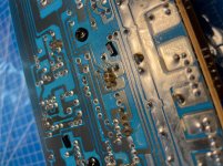
Looking at the back of the boards, there is some white/tan residue. Is this just leftover from the soldering process? There is also a lot of brown stuff around some joints - leftover flux?
Could either of these allow current to flow between joints where it shouldn't?
Thanks!
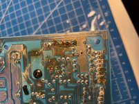
Most of that looks like residue from resin/flux. Although in the 2nd picture, there seems to be some overheating marks from a component. Worthy of checking the component.
Best to clean that up resin/flux with IPA and check those joints (cold?) as well.
adding picture for over-heated component

Also looks like a cold or cracked solder joint.
Last edited:
The zener diodes especially are all over the place. .
IMO zeners are definitely best checked with power applied. If they are not holding the spec'd voltage time to replace.
Typical fast switching silicon diodes (1n4148) are cheap. If in question just replace.
For the silicon diode .7V forward drop is good, less than .7V I'd start thinking about replacing.
Resistance-wise in a forward bias probing, I'd expect something smaller than megohms...or were the leads reversed?
As for zener checking, since you have the boards out of the chassis, can you build a proto-type circuit with the zener? A small 20+ DC power supply, a series dropping resistor (1Kohm) and the zener....see if the zener works.
Last edited:
IMO zeners are definitely best checked with power applied. If they are not holding the spec'd voltage time to replace.
Typical fast switching silicon diodes (1n4148) are cheap. If in question just replace.
For the silicon diode .7V forward drop is good, less than .7V I'd start thinking about replacing.
Resistance-wise in a forward bias probing, I'd expect something smaller than megohms...or were the leads reversed?
Megohms with leads in both forward and reverse bias on the zeners.
I ordered replacements for all diodes - they're so cheap there was no reason not to.
Most of that looks like residue from resin/flux. Although in the 2nd picture, there seems to be some overheating marks from a component. Worthy of checking the component.
Best to clean that up resin/flux with IPA and check those joints (cold?) as well.
adding picture for over-heated componentView attachment 998504
Also looks like a cold or cracked solder joint.
There are definitely overheating marks on a few places on the boards. Nothing major though. I've checked all those components (all resistors) and they measure in spec.
The area you circled is a big resistor that sits about 4mm above the board. The joint is ok - I had to put extra solder there for more support because the trace was coming off the board. Actually all four of the resistors in those positions on each board are like that. Subpar circuitboards I guess. I've measured the joint to ensure a good contact with the resistor itself and the next component on the trace.
OK, it just looks bad in the pic. Just be certain there's no "wiggle" when pushing on the resistor lead. FWIW, I'll remove all solder then reapply with 60/40 on a difficult joint.
There are 2 joints below the screw head that also have the "look" of a bullseye or broken joint.
Most of that looks like residue from resin/flux. Although in the 2nd picture, there seems to be some overheating marks from a component. Worthy of checking the component.
Best to clean that up resin/flux with IPA and check those joints (cold?) as well.
adding picture for over-heated componentView attachment 998504
Also looks like a cold or cracked solder joint.
There is an art to soldering which takes a while to get right.
Since we have youtube demonstrations on any subject you can name I will leave that of soldering for others to research.
- Home
- Amplifiers
- Solid State
- NAD C370 help pls