NAD 3125 Integrated Amplifier
This unit immediately blows 4A fuses F1 and F2 upon powerup.
Even with F1 and F2 blown I get some output, but extremely distorted.
Preamp circuit appears OK.
Main amp bridge rectifier pulled and tested OK.
Main amp large 4700uF 50V filter caps pulled and tested OK.
I disconnected output transistors Q110/Q210 and Q111/Q211
Now the fuses don't blow and I get clean +27V and -27V on the output power rails. Good!
I then pulled and tested all four output transistors (D1148R and B863R) and they appear OK. C to E is not shorted. Testing with the DMM on diode check mode and each transistor looks like a pair of diodes, just like one would expect for an NPN and PNP bipolar transistor.
I then pulled and tested another small transistor Q107/Q207 and they also appear OK. This transistor is mounted on the heatsink either for cooling or temperature compensation. I believe this transistor is part of the bias adjustment circuit.
I don't see any discolored or burnt components anywhere.
Any suggestions for what to check next?
I don't have the 3125 schematic but the 7125 appears to use the same circuit and reference designators.
https://www.vintageshifi.com/repertoire-pdf/pdf/telecharge.php?pdf=Nad-7125-Service-Manual.pdf
Last edited:
I had a amp tonight take loads of current.
So I find simplest way to debug is to remove outputs and feed output base resistor back into ltp. The amp will then power on with feedback and you can measure all voltages and bias voltage for errors.
In my case it was a silly where I had wired bias pot wrong way around and on min setting was getting 1 amp bias current ! Turned the pot right way around now works a treat.
Dont do what I did on a previous fault. I fixed the blown transistors and they just blew again after a minutes use.
I had fried the speaker and it was very low impedance and blew the amp again.
The service manual makes mention of two adjustments in the power amp section: CENTER VOLTAGE and IDLE CURRENT.
The pots for setting the idle current are set to about the same value, but the pots for setting the center voltage are very different, maybe a previous owner was in there twiddling things around.
Is "center voltage" the same thing as bias adjustment? And if it was set improperly could it cause the output transistors to draw too much power from the output power rails, blowing the fuses?
Going through and checking diodes and transistors in the amp section, still have not found anything open or shorted. Weird.
I'll try to rig up a dim bulb tester and solder the output transistors back in to see if I can uncover any more clues.
I recommend a Iceo test on the output transistors before putting back in. Damaged transistors can resist 2 v of a DVM, but not 40 volt rail.
I found bad ones with a 12 v battery charger, series a 47 k resistor and ma scale of a DVM. Plus goes to C of npn, minus goes to E. Base open. Opposite polarity on pnp. Current=12/47000, your transistor is leaking. Current <2 microamp, it is fine. 12 v wall transformers are probably cheaper than a car battery charger, but you have to find a mate for the barrel connector.
Center voltage is for setting Vout with inputs shorted at zero.
Last edited:
Thanks for the suggestion. I checked Iceo for all four output transistors and observed no current flow up to 17V which was the limit of my bench supply. I then double checked the b-e and b-c junctions with my DMM and all output transistors look OK to me.
It's strange because the power rails that are showing excessive current draw only go to a few places, and as far as I can tell, all of those components are working OK.
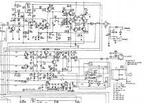
BTW, here is the schematic for the NAD 3125. It's hand drawn and barely readable but it's possible to follow it.
It's strange because the power rails that are showing excessive current draw only go to a few places, and as far as I can tell, all of those components are working OK.
BTW, here is the schematic for the NAD 3125. It's hand drawn and barely readable but it's possible to follow it.
Output transistors Q110 and Q111 removed from circuit.
The trace going to the base of Q110 and Q111 is -28V
Base of Q108 and Q109 is -28V
Base of Q107 is -28V
Seems like something is up in the bias circuit. With no speakers and no inputs connected, I would think that the bias should be at least different for the pull up and pull down transistors. Seems like something is shorting the base of these transistors to the negative rail of the output power supply.
So what is the voltage at the emitter of Q>4, the VAS? same point as left side of C124.
What is the voltage at bk01, which is supposed to be zero quiescent?
What is the voltage at bk01, which is supposed to be zero quiescent?
Sorry, I'm not sure what transistor you're referring to "Q>4" and I'm not sure what "VAS?" means.The negative pin of C124 is grounded, and the positive pin has 0V on it. The voltage at BK101 is zero, but that is expected as the output transistors have been removed.
I could try to put the output transistors back in, but I may blow my last 2 T4A fuses if I do. I've got a 40W dim bulb tester inline with the power.
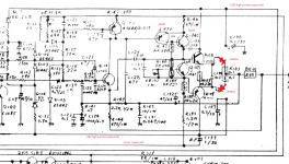
(The awful hand drawn PDF schematic I posted is the correct, the image I posted earlier is for a different board and some of the reference designators are different.)
I could try to put the output transistors back in, but I may blow my last 2 T4A fuses if I do. I've got a 40W dim bulb tester inline with the power.
(The awful hand drawn PDF schematic I posted is the correct, the image I posted earlier is for a different board and some of the reference designators are different.)
You are the one that posted that fuzzy awful print. C124 at least the one I read as c124, doesn't have plus or minus ends. So, no data. The blocking cap connected to the emitter of the VAS which reads as "Q->4" which is absurd. the question is, how does -28 v get to the base of the lower output transistors? I don't see any way for it to get there unless some part not a usual suspect failed.Sorry, I'm not sure what transistor you're referring to "Q>4" and I'm not sure what "VAS?"
If I had a 40 w bulb in series with the AC, I'd replace the 4 A fuse with 15 A AG3 fuse from the auto supply while I took some voltage readings. O-Reilly's had AG3 fuses last time I was in there, cheaper than newark.
You do know about not using both hands while the power is on, don't you? 24 v from one hand to the other can stop your heart. No rings or jewelry on hands, wrists, neck. 1 v @ 30 amps can burn your flesh to charcoal. Connect black probe of DVM to speaker ground with an alligator clip lead. Wear safety glasses, parts sometimes explode. I blew the top off some TO3 metal cans once, bounced off the ceiling.
Last edited:
Yeah, I know that schematic sucks. If a better copy of the NAD 3125 schematic exists anywhere I've not been able to find it and I've spent a long time looking.
It looks like Q104 is the transistor and C129 is the 100pF blocking cap. The emitter of Q104 is at 0.7V. You're right, it still doesn't explain how the -28V is getting on the bases of Q107, Q108, Q109, Q110 and Q111. And the other channel is exactly the same.
At this point I'm out of ideas for components to test, so I'll put the output transistors back in, replace the 4A fuses with beefier ones, and use the 40W dim bulb on the mains and see what smokes.
It looks as if the junction of R151 and C135 is the negative rail, so without the output transistor in there -whatever the rail is goes through r130 to the base of Q109. So that is not a problem. When Q109 is there the b-e junction should force that point to a much higher voltage.
R's147 and 148 are what's pulling down on the entire output section, sans outputs. 1k2 each, coming from the minus 'super-rail' -- not the high current supply for the output-transistors-proper.
If you're determined to continue analyzing, you'll need to find a reasonable place/way to close the feedback loop -- that would be Output (both sides of 'BK101') to R140 and R142 on the partial schematic posted earlier (post 2). Fit a couple general purpose rectifiers, 1N4004 or the like, forward biased in place of the Base-Emitter junctions of the output transistors. Jumpers and tack-soldering are OK.
The VAS (Q105, Q106) is the only thing pulling toward the positive rail. Without the feedback loop it will remain off and R147 and R148 will be in charge.
If you don't close the feedback loop, none of the voltages will seem reasonable.
Cheers
Last edited:
Thanks Rick. I see what you mean about those two resistors pulling everything down to the minus 'super rail'. Looks like there is already a feedback path from either side of BK101 to R141 and R143. (The snippet in post #2 is for a different product.) I'll try adding a couple of diodes in place of the output transistors as you suggest and then re-check voltages in the amp stage.
Attachments
You're welcome! 😀
Wish I could've thought of a better name than 'super rail' -- that term is usually reserved for a pair of rails, lower-current but a few volts higher, than the rails serving the outputs. It improves linearity and output peak-to-peak voltage capability.
I take it back. Now that I'm looking at the correct schematic, they do appear to be just that. Yay.
Cheers
Fuse blow
Possibly one or more diodes of the bridge rectifier at F1/F2 is shorted, causing a full short of the transformer at one or both halves of the sinewave.
Possibly one or more diodes of the bridge rectifier at F1/F2 is shorted, causing a full short of the transformer at one or both halves of the sinewave.
I pulled that bridge rectifier and it tested OK. The +28V and -28V rails look great and the fuses don't blow as long as all 4 output transistors are removed. Tonight I'll do the mods Rick mentioned (post #15) and report back on what I find. Hopefully by comparing L and R channels I should be able to find something unusual.
I pulled the output transistors and they passed every test I could think of. I just don't see any shorts and I tool Vceo up to 17V. But if I do need to replace them, are these (B863 and D1148) things unobtainium? It sounds like the ones for sale on eBay are fakes.
I pulled the output transistors and they passed every test I could think of. I just don't see any shorts and I tool Vceo up to 17V. But if I do need to replace them, are these (B863 and D1148) things unobtainium? It sounds like the ones for sale on eBay are fakes.
- Home
- Amplifiers
- Solid State
- NAD 3125 blown fuses and output transistors