Okay so wanted to see what sort of stability margin we're working with with the stock compensation and lm318 etc just as a baseline, so plugged it into scarlett 2i2 interface, with 1:10 attenuator, and for load a 100W 4 ohm resistor (inductor really), cables are short and normal.
Sine wave we get to about 10vrms and then it oscillates, and when i say oscillate i mean not only electrically but litterally makes sound physically, becomes a buzzer, this is like in a split of a second. Actually i didnt even need the interface, could have just used ear.
For multitone, it starts buzzing and oscillating at around 1Vrms only., here is pic right before it happens ( i just noticed i didnt capture scales, well, that makes it a bit useless..). Also the linearity is weird, HF seems increased.
If multitone is in any way representative of music, then 1Vrms is pretty low so cant really plug this in nice speakers..dunno what's wrong with mine.
One thing that stood out to me when hooking it up to the scarlett, i checked the potentials between terminals with it playing nothing, grounds (black plugs) are at identical potential, but the hot leads differ by 0.365V DC.
Not sure what's up with that, probably not healthy. One time i plugged it into a TPA3116, and with only 1 lead, ground lead connected, it heated up the resistor to where i could barely touch it. So it somehow closed the loop though that "ground" connection and it all went through my interface and somehow everything survived...but that's a story from the past.
oi.
wait.
something is wrong, this amp is rock stable, full volume, even into hard clipping.. Just pointing out, before somebody would start to think wrong..
What do you mean by inductor?
wait.
something is wrong, this amp is rock stable, full volume, even into hard clipping.. Just pointing out, before somebody would start to think wrong..
What do you mean by inductor?
ok.. start to understand some things
the topology includes a "soft clipping scheme", which limits at the zone of 28V/ 28,5V Vpeak. (so it is 56V/57Vpeak-peak, that is cca 20Vrms)
But!! that limit is defined by the zener diode in the limiter scheme. For this to work, one needs that the amplifier, the LM3886 chip itself should still be safely clear of it's own rails, far from clipping when the limiter scheme enters in function. Basically, the limiter scheme to properly work, one needs the original prescribed rails, +_36V DC...
You are operating the amp at +_23V, that is +_13V below it's proper, +_36VDC rails prescription..
So the limiter scheme does not work, and it generates quite a chaos when driven in clipping..
The other point is, that with a single current pump I have noticed that proper, high quality output with low distortion disrupts at about 14Vrms with 4 ohm load.. (instead of the full swing, 20Vrms output)
Now, this could be different with your low rails setup, but again: with +_23VDC rails I would expect clipping already below /at max. around 14Vrms, on 4 ohm load..
Now, this could be different with your low rails setup, but again: with +_23VDC rails I would expect clipping already below /at max. around 14Vrms, on 4 ohm load..
Last edited:
So.. these are just hints, I am not sure that this is what happens really. Your 1Vrms result is for sure not explained..
Hello, thanks for your replies George
Do you think a NOS dac with only first order analog filtering could also contribute to earlier oscillation, due to its aliasing images?
Mind you, i used the outputs of the 2i2 which im sure has a steep filter, so i guess that isnt it here.
Hmm....
I was reading @tomchr 's articles on this, i decided to build a TINA schematic (since LTspice wasnt really working for LM3886 model, for some reason), and test around the phase margin and check around, since there doesnt seem to be an explanation anywhere of how certain values were chosen for the My_ref, or its buried in 300 pages, or pretty "high level" (i.e overview) info. Unfortunately LM318 doesnt have all pins implemented but i guess its something to get started..

I got it to work but not sure where to put the inductor so its closed at DC but open at AC, for AC analysis. Tried around different things but nothing seems to give a realistic result, i.e phase margin is already below 0 from the get go..
Well...you know how those large generic wirewound resistors are wound...they're very inductive is all i meant. I guess speakers are inductive loads as well so it might not be a bad thing to test worst case.What do you mean by inductor?
That's a very good point, it wouldnt have occured to me...You are operating the amp at +_23V, that is +_13V below it's proper, +_36VDC rails prescription..
So the limiter scheme does not work, and it generates quite a chaos when driven in clipping..
Okay, so 14vrms, i guess 10 for sine isnt that far off but yeah the multitone is hard to explain..The other point is, that with a single current pump I have noticed that proper, high quality output with low distortion disrupts at about 14Vrms with 4 ohm load.. (instead of the full swing, 20Vrms output)
Now, this could be different with your low rails setup, but again: with +_23VDC rails I would expect clipping already below /at max. around 14Vrms, on 4 ohm load..
Do you think a NOS dac with only first order analog filtering could also contribute to earlier oscillation, due to its aliasing images?
Mind you, i used the outputs of the 2i2 which im sure has a steep filter, so i guess that isnt it here.
Hmm....
I was reading @tomchr 's articles on this, i decided to build a TINA schematic (since LTspice wasnt really working for LM3886 model, for some reason), and test around the phase margin and check around, since there doesnt seem to be an explanation anywhere of how certain values were chosen for the My_ref, or its buried in 300 pages, or pretty "high level" (i.e overview) info. Unfortunately LM318 doesnt have all pins implemented but i guess its something to get started..
I got it to work but not sure where to put the inductor so its closed at DC but open at AC, for AC analysis. Tried around different things but nothing seems to give a realistic result, i.e phase margin is already below 0 from the get go..
You're not looking at the phase margin in your simulations, though. You're looking at the closed loop gain/phase. Just saying.
Tom
Tom
Thanks for that Tom, reading Cordell's book now, just trying to figure out where i can learn this as i narrowly took the software path in life instead of EE. Gotta figure out how to make an open loop AC measurement, use TINA, while having a day job and obligations... Think might have done the trick though..You're not looking at the phase margin in your simulations, though. You're looking at the closed loop gain/phase. Just saying.
Tom
EDIT: hmm no maybe not, i can delete or add a large amount of stuff (like cap across lm3886 inputs (Cc)) with no change to the phase at all..
Last edited:
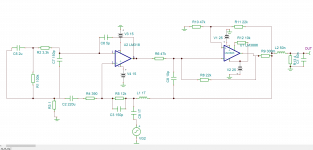
Most of the schematic is obscured by the graph. I'm not sure how you expect anybody to help.
Tom
Tom
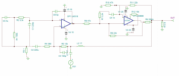
I made sure that the only change, the 1T inductor on the output of the LM3886 is visible (ok, the input cap is back to 4uF since it didnt make a difference). Other than that it's the same schematic as 1 post, and 2 posts above. You're right, sorry maybe should have noted that in the post... I didnt want to make it too image heavy by posting more images than necessary since this encodes all the information (given the context that what is not visible is untouched, which i failed to mention..) there's also an .asc available to anyone to test around with 1 post above, since it would be unreasonable (and unecessary!) to have people remake it from scratch, and also helps people viewing this in the futureMost of the schematic is obscured by the graph. I'm not sure how you expect anybody to help.
Tom
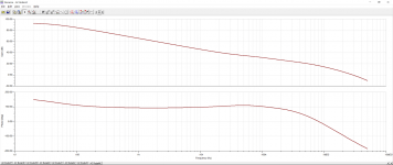
really the graphs are not interesting, they are just measuring the wrong parameters.. so turn them off, show the full circuit.
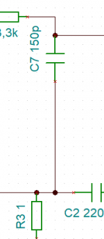
You have inserted that inductor in the wrong place. At that point You interrupt a local feedback loop of the Howland current pump.
You have to 'disrupt' with the inductor the global feedback loop.
A good place to do that would be to disconnect from the output node the 12kohm feedback resistor (global feedback) and insert there the 1T inductor.
Then, you have to disconnect the signal generator VG1 from where it is now (input). in place of the VG1, place a short circuit on/ across the original input node.
Now You have interrupted the global feedback for all dynamic excitations, only the DC connection is established.
Now You can measure the loop gain from the input of the global feedback network (12kohm upper end, 1TH side) across feedback network (Beta) and the composit gain of all the active elements (A1*A2)right up to the output node(the output node side of the 1TH inductor).
To be able to compute this, you have to move the VG1 signal source to this new test input, the common node of the 1TH inductor & 12kohm feedback resistor.
You need to place a capacitor in series to the sig. gen, so as not to influence the DC balance.
GND - VG1 - 1Farad cap - 12kohm/1T
Your test point for gain and phase remains the Vout. (on the other side of the 1T inductor)
I did not make the scheme, on purpose.. 🙂 🙂
Last edited:
Thanks a lot guys! Dont think i would have figured it out without your help, so i appreciate it.


Then with the compensation cap (5p from non inverting to output in this case)


Phase margin is improved, at the cost of some gain 🙂


Happy Easter ! (i guess a little late 🙂 )
Without compensation capacitorreally the graphs are not interesting, they are just measuring the wrong parameters.. so turn them off, show the full circuit.
You have inserted that inductor in the wrong place. At that point You interrupt a local feedback loop of the Howland current pump.
You have to 'disrupt' with the inductor the global feedback loop.
A good place to do that would be to disconnect from the output node the 12kohm feedback resistor (global feedback) and insert there the 1T inductor.
Then, you have to disconnect the signal generator VG1 from where it is now (input). in place of the VG1, place a short circuit on/ across the original input node.
Now You have interrupted the global feedback for all dynamic excitations, only the DC connection is established.
Now You can measure the loop gain from the input of the global feedback network (12kohm upper end, 1TH side) across feedback network (Beta) and the composit gain of all the active elements (A1*A2)right up to the output node(the output node side of the 1TH inductor).
To be able to compute this, you have to move the VG1 signal source to this new test input, the common node of the 1TH inductor & 12kohm feedback resistor.
You need to place a capacitor in series to the sig. gen, so as not to influence the DC balance.
GND - VG1 - 1Farad cap - 12kohm/1T
Your test point for gain and phase remains the Vout. (on the other side of the 1T inductor)
I did not make the scheme, on purpose.. 🙂 🙂
Then with the compensation cap (5p from non inverting to output in this case)
Phase margin is improved, at the cost of some gain 🙂
Thank you, here's the scheme and result i got for this setup, not sure if something needs to be changed.Another good spot for breaking the loop is at the output of the LM318 (assuming the schematic of Post 4926).
Tom
Happy Easter ! (i guess a little late 🙂 )
Attachments
duh.. first of all-
Yes, You had made nice progress, congratulations!
Now things start to work. (I mean the simulation.. 😂 the circuit do not seem too much so.. 😜)
The second part, with Tom's suggestion, is not giving You the correct loop gain, though. You just see the gain of the LM3886 current pump (working into 8ohm)
the first part, placing the loop break point at the output, does work. ~+_.....
but I do not like the result, the curves that You get.
I lost some time until I started to be able to reproduce Your result. I get a similar output, If I disconnect the noise gain compensation network on the input of the LM3886... 🤔🙄 (R7, C4)
it looks like R7, C4 would be disconnected from your circuit..
That double point between R10, R11 do not look like normal..
Then: the stability requirement is that at the point where the loop gain magnitude is reaching 0dB (unity gain) in the Bode plot, at that crossing frequency the phase plot should still stay above 0 degree.. (it started from +180 degree at 0Hz)
" if the loop gain’s magnitude is less than unity at the frequency where the loop gain’s phase shift is 180°, the circuit is stable. In practice, the loop gain must be significantly less than unity at this" frequency to avoid marginal stability."
This is not fulfilled in your sims.. so there is a problem.
An other possibility for cross-check is to reinstall the original circuit, - remove the loop breaking 1TH inductor, place back VG1 properly at the input..
define VG1 like a : square wave; 600mV amplitude; frequency 10k; rise / fall time 50nsec
And try to run a transient analysis.
Good luck! George
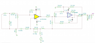
my suggestion is that try to clean up that network. Eliminate all the wires, leave only the components, and redo it in a clean way. (R10;R11, R7, C4, lm3886)That double point between R10, R11 do not look like normal..
Thank you! Thanks to you 🙂duh.. first of all-
Yes, You had made nice progress, congratulations!
Sorry i did not respond earlier to your help, only now found a block of time to gather my thoughts and process all of it
Seems to me as well..Now things start to work. (I mean the simulation.. 😂 the circuit do not seem too much so.. 😜)
The second part, with Tom's suggestion, is not giving You the correct loop gain, though. You just see the gain of the LM3886 current pump (working into 8ohm)
You're right, my bad. But looks like it did not bother TI. At least it seems to see the connectional representation the same, as the output result is the same. I removed it now.. actually i redid all the connections on the whole thing as you suggested because and it's an excellent suggestion, TINA seems to be a bit more finnicky with making connections than what im used with in LTspice. I noticed this difference.the first part, placing the loop break point at the output, does work. ~+_.....
but I do not like the result, the curves that You get.
I lost some time until I started to be able to reproduce Your result. I get a similar output, If I disconnect the noise gain compensation network on the input of the LM3886... 🤔🙄 (R7, C4)
it looks like R7, C4 would be disconnected from your circuit..
That double point between R10, R11 do not look like normal..
Schematic now looks like this (also zipped as attachment)
Then: the stability requirement is that at the point where the loop gain magnitude is reaching 0dB (unity gain) in the Bode plot, at that crossing frequency the phase plot should still stay above 0 degree.. (it started from +180 degree at 0Hz)
" if the loop gain’s magnitude is less than unity at the frequency where the loop gain’s phase shift is 180°, the circuit is stable. In practice, the loop gain must be significantly less than unity at this" frequency to avoid marginal stability."
This is not fulfilled in your sims.. so there is a problem.
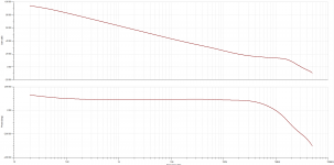
The phase now looks even worse after the fix, but lets see...
Ok, so we have the 0db point on the Bode plot at 3.72Mhz, at that point the amp should still have a phase margin to work with, yet its out by 1.16Mhz. Oscillation!
An other possibility for cross-check is to reinstall the original circuit, - remove the loop breaking 1TH inductor, place back VG1 properly at the input..
define VG1 like a : square wave; 600mV amplitude; frequency 10k; rise / fall time 50nsec
And try to run a transient analysis.
Good luck! George
Yes, oscillates like wild, will need to investigate this further. But schematic seems correct, so i wonder if its just the models?
Attachments

Hi all,
My board from 15th group buy. All smd already fitted, plus some 0.6w resistors on top of the board.

I am thinking how to connect the AC 230V lead to the transformers (these have leads only 15 cm long) to reach the rear panel.
My board from 15th group buy. All smd already fitted, plus some 0.6w resistors on top of the board.
I am thinking how to connect the AC 230V lead to the transformers (these have leads only 15 cm long) to reach the rear panel.
- Extend AC 230V leads through terminal blocks
- Insert a softstart module between the network connector and the transformer.
- Home
- Amplifiers
- Chip Amps
- My_Ref Fremen Edition - Build thread and tutorial