
By 80, playing with new turn table and tone arm design will be my main indoor toy. Already have some concepts in my mind and probably will be doing some trials for proof of concept. I have seen some good stuff out there, but none really catches my heart.
I've asked Penasa about the mods
I received Mauro's opinion about the C9-R10 mod and about R11.
C9-R10:
No problems about it and actually it can reduce picked up noise but he's not sure that a subjective improvement can be heard; it's also possible that, subjectively, things go worse.
I'll give it a try in the WE.
R11:
It's needed and improves noise rejection from GND by several tens dB.
It will stay on board and BOM.
Obviously every builder with a different opinion is free to jumper it... 😉
Last edited:
For me, R11 became a fuseable link when I hooked up a preamp that I had powered wrong.
With the new LM3886 grounding probably it's no longer so.
We have a last minute new partecipant: romvise (Italy) 🙂
Ready for production?
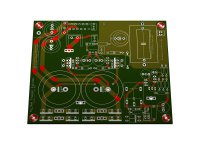
I've quite finished the optimization and refinement of the PCB:

This layout includes the C9/R10 mod (I'll try it Saturday/Sunday).
Any comment?
I've quite finished the optimization and refinement of the PCB:
This layout includes the C9/R10 mod (I'll try it Saturday/Sunday).
Any comment?
Attachments

The small arrowheads on the bottom correspond to polarity by reading the lettering from left to right - correct?
The small arrowheads on the bottom correspond to polarity by reading the lettering from left to right - correct?
Exactly.
I've yet to verify howland pump resistors orientation.
The PCB is also optimized on most pads with round corners, smooth transitions and some teardrops according to Metal's suggestions.
I've also received from Suburra confirmations on most polarities and BOM choices.
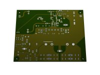
The Google folder has been updated with all relevant files and BOM which includes the modified C10 (from SMD to TH).

Latest PCB layout.
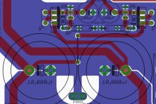
KSTR asks whether the speaker cabling loop area has an effect on the sound quality.
I will guess a "yes" answer to that.
Look at the OUT terminal. It has a lot of space around it and it has a Ground Plane right next to it.
Move the OUT terminal to the right to use that spare space to the right.
Fill the now empty space to the left with your extended ground plane.
Solder a Speaker Ground Terminal (Speaker Return) in that new ground plane close to the OUT terminal.
Now listen to the two versions. One using the original Speaker Ground Terminal on the relay section of the PCB and this new version with the OUT and Return next to each other.
If the builders agree that the Speaker Return sounds better than the Speaker Ground Terminal you can look at moving the relay to the Speaker Return area.
Last edited:
The small arrowheads on the bottom correspond to polarity by reading the lettering from left to right - correct?
To make sure I understand, if I am looking at a surface mount resistor and the label says 220, the arrow on the board points from the 2 toward the 0. Do I have it correct?
Jac
It looks like a jumper is under C101. If so, it really should be moved, maybe like this:
It's pretty easy moving it:
But I would like to understand why you think it's better to move it, because it's on the ground return path?
Can you elaborate a bit?
Thanks in advance
KSTR asks whether the speaker cabling loop area has an effect on the sound quality.
I will guess a "yes" answer to that.
I guess it's possible...
Look at the OUT terminal. It has a lot of space around it and it has a Ground Plane right next to it.
Move the OUT terminal to the right to use that spare space to the right.
Fill the now empty space to the left with your extended ground plane.
Solder a Speaker Ground Terminal (Speaker Return) in that new ground plane close to the OUT terminal.
Something like that, right?
It's nice idea but it could be a bit misleading... in practice it's a DC protection bypass...
If the builders agree that the Speaker Return sounds better than the Speaker Ground Terminal you can look at moving the relay to the Speaker Return area.
Doing that move would imply that the output trace going to the DC protection circuitry would necesarily cross PS traces, is it a good idea?
None of the My_Ref PCBs, including the MY_Evo, do that.
if I am looking at a surface mount resistor and the label says 220, the arrow on the board points from the 2 toward the 0. Do I have it correct?
Exactly 😉
Attachments

Compare the new Return location to the old Ground location, FIRST.
Then decide if the relay needs to be moved !!!!!
If it turns out that KSTR's concern is well founded, the relay can be located any where on the PCB, or even off the PCB and you just run a pair of wires/traces from the detect and trigger circuit to the new relay location. What else are you thinking about? I can't imagine.
Compare the new Return location to the old Ground location FIRST.
Then decide if the relay needs to be moved !!!!!
I do agree that having speakers ground return in this new position would probably be both neater and in general better.
Nevertheless the beta PCBs sound great.
If it turns out that KSTR's concern is well founded, the relay can be located any where on the PCB, or even off the PCB and you just run a pair of wires/traces from the detect and trigger circuit to the new relay location.
The only viable solution, IMHO, would be the external DC protection, we talked about it also in design phase.
By now it's a bit to late, probably we should wait Klaus'tests to verify if it's really a problem or not before doing such a radical layout change.
Release Candidate boards will ship with the classic DC protection on board.
We will approach again the possible problem in a future 'Fremen Edition II' but, maybe, I'll introduce a new approach to the DC protection based on MOSFETS instead of relays. 😉
I'll get back on my soapbox again buy saying thanks to all who have contributed new and valid ideas to enhance the performance of the Fremen Edition. A subsequent version looks very promising indeed.
IMHO, let me suggest that getting this BOM and PCB into the hands and systems of as many builders as possible now, will only give more validity and agreement on future changes. There is always that ever present "why should I do this when a better one might appear?". That's a personal choice, but let me suggest nothing will replace hands-on experience and field testing for zeroing in on significant improvements. Six to eight months (or more) of the kind of interactions that have occurred in the last several weeks sounds like a very exciting prospect to me.
IMHO, let me suggest that getting this BOM and PCB into the hands and systems of as many builders as possible now, will only give more validity and agreement on future changes. There is always that ever present "why should I do this when a better one might appear?". That's a personal choice, but let me suggest nothing will replace hands-on experience and field testing for zeroing in on significant improvements. Six to eight months (or more) of the kind of interactions that have occurred in the last several weeks sounds like a very exciting prospect to me.
It's pretty easy moving it:
But I would like to understand why you think it's better to move it, because it's on the ground return path?
Can you elaborate a bit?
It's a mechanical issue, not related to the electrical layout. The version with the jumper under C101 requires that in assembly the jumper must be installed before C101. The jumper wire must be trimmed flush with the top side of the board so the wire does not touch C101. Then the area around the jumper vias on the top side of the board needs to be cleaned with alcohol.
All this can be avoided by just moving the jumper. Then solder flux will not be trapped under C101 and the jumper cannot poke a hole in the bottom of C101. It's good practice to avoid placing vias under components, especially capacitors.
It's a mechanical issue, not related to the electrical layout.
(...)
It's good practice to avoid placing vias under components, especially capacitors.
Thanks, now it's clear 🙂
I'll get back on my soapbox again buy saying thanks to all who have contributed new and valid ideas to enhance the performance of the Fremen Edition. A subsequent version looks very promising indeed.
Maybe it's not clear but I appreciate (and often make some use of) every comment. 😉
In fact, thanks to Andrew's comment, I realized that there were space for optimizing the PS traces and ground plane near the LM3886.
Last edited:
I'll get back on my soapbox again buy saying thanks :
In the third grade Mrs. Haffy told me to put more time on my spelling workbook. Sometimes we see what we think and not what we type.😱 Those da*m spell checkers can't read my mind either.😀
- Status
- Not open for further replies.
- Home
- Amplifiers
- Chip Amps
- My_Ref Fremen Edition - Beta build/Fine tuning