May I suggest an interest check thread prior to ordering the PCBs? These may go faster than you think! 🙂
May I suggest an interest check thread prior to ordering the PCBs? These may go faster than you think! 🙂
I'd be interested in a couple.
I will be interested in 4 positive/negative boards ( assuming single board contains one positive and one negative?)
The board shown has only one poitive or can be used as negative or positive ?
kannan
The board shown has only one poitive or can be used as negative or positive ?
kannan
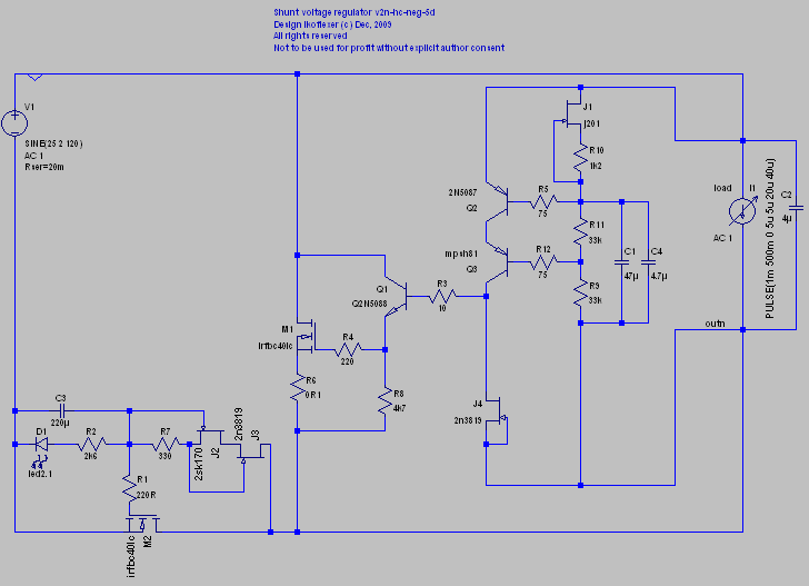
Oh, the negative version  Didn't think there would be so much interest in it. OK, more work needs to be done then. The circuit design I have done some time ago, and even built a negative prototype. Will report progress as it happens. The wheels on the bus go round and round ...
Didn't think there would be so much interest in it. OK, more work needs to be done then. The circuit design I have done some time ago, and even built a negative prototype. Will report progress as it happens. The wheels on the bus go round and round ... Here's the sneak preview negative version circuit for those who want to build it on their own. Pretty much all the comments from the positive version apply. I decided some time ago not to go with complementary devices (i.e. instead of n-channel mosfets to use p-channel mosfets, etc.). Instead the topology is turned upside down 😀 but the benefit is that you can expect a much closer match in terms of performance for the positive and negative rails, plus, using the same devices in both circuits makes it easier when shopping around for components.
This will be revision 5d. The only changes from 5c is using only one LED in biasing M2, and the addition of capacitor C4, which is intended to be a film type, or whatever. This position seems to be important and several people have mentioned that the type and value makes an audible difference. Look back in the thread for hifinutnut's comments, it'll be helpful (thanks hifinutnut!).
REMINDER: all capacitor and resistor value are not intended to be exact values. 1% tolerance is not what this circuit is about and it would make no difference in reality. Some resistor values shown in the circuit MUST be changed according to the parts that you end up with. It is possible to narrow the values down, but well, do you want a few pages of math? It's much easier if I give you a recipe, and I'm going to write one.
Example: the CCS mosfet M2 limits the main current output. Now, you can use a lot of different mosfets for M2. Some people may not like this, but I like it. I've always liked to have options AND a default that is well chosen. In this case I chose the default to be irfbc40 or irfp240, both will work like a charm. But hey, maybe you have an irf630 on hand. It can be used just fine. But each may be biased slightly different. So we use a mini-CCS (constant current source) to pass a relatively constant current through R2 and the LED. Both the LED and R2 cause a voltage drop. It could be about 2V across the LED, and another 1.5V across R2, depending on its value and the current passing through it. The total voltage across LED+R2 is the same as the voltage that M2 has at its G and S pins. But this works well if we pass a certain relatively constant current through D1+R2. That is achieved via the mini-CCS made up of J2, J3, and R7. I won't go into details, but there is theory that says you get good regulation (and tempco) in a CCS by using a value of R7 such that the current limit of this mini-CCS be about 15% of the Idss of J2. When I say "about" it means approximately. No need to go crazy here with exact measurements because it won't make a difference. So hook up J2 in series with a 3V battery and your DMM in series, set on 20mA. J2 G and S pins touching. J2 D pin on +3V. G+S on V+ probe of DMM. -3V on V- probe of DMM (in the how to I'll draw a picture 😉 ). This is how you measure Idss of J2. Let's say it is 10mA. Good, 15% of 10mA is 1.5mA. Now hook up J2 + J3 + 500R trimmer as shown in the circuit, to a 3V battery in series with your DMM set on 20mA. Adjust the trimmer until your DMM shows 1.5mA. Take the trimmer out and see how many ohms it measures. It could be 200 ohms. Find the closest fix value resistor you have. Don't obsess about a few tens microamperes difference. I know it's hard not to obsess for an audiophile, but you have to try. That's how R7 value is decided. This is the recipe. Then, in the real circuit you'll use this R7, and you will use a trimmer for R2 to get the current limit that you want. Then replace the trimmer with a fix value for R2.
Now, back to the drawing board for me get that negative rail pcb done. 🙂
Cool, thank you telstar 😎
Oh, talk about progress, a tiny bit of progress here, to allow the pcb to take the bypass film cap. Here it's hard to satisfy everybody, because there will always be some gynormous cap size that it's hard to fit, but nevertheless...
Edit: I left the two LED footprints in because it's easy to shunt one. There might be some people who want to use two 1.7V Vf LEDs, and then use a very small value for R2.
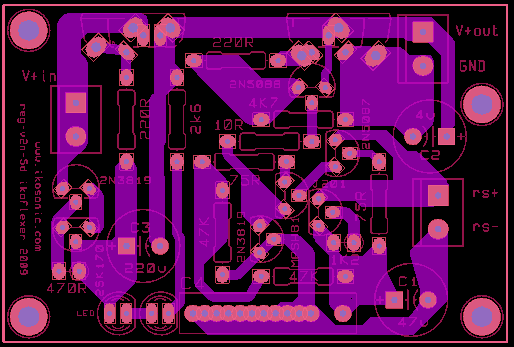
Last edited:
OT: salas, I'm on my way out with my wife, to Greek town, to get the best spanakopita in the city 😀 courtesy of your many country men that live here 😀
After extensive testing of this regulator, some conclusions:
According to Siliconix Application note AN103: LINK
and Walt Jung research on CCS, Figure 8A: LINK
appears, that optimal working point for cascoded CCS (J3 and J4) should be Vdg = 2*Vgs(off). This rule is valid for both devices.
2SK170 Vgs(off) = 1.5V (max), but 2N3819 Vgs(off) = 8V(max).
If we apply this formula to 2N3819, then 2*8V = 16V between Drain and Gate. If current through R7 is 500uA, then voltage drop on resistor is 0.375V.
For biasing M2 MOSFET's gate we need 4.5V (Vgs threshold voltage) or more for higher current.
All together, input voltage should be 20V or more higher than output voltage for optimal working cascode.
I think it is better to replace 2N3819 with other JFET with lower Vgs.
Attachments
Last edited:
Good points stormsonic. I would like to say that there are two things to consider. One, the 2n3819 is not a device separated in levels like the j201, j202, and j203, or the 2sk170gr 2sk170bl and 2sk170v. What this means is that the 8V max Vgs(off) is only a max; when you buy some 2n3819 they may have a Vgs(off) of 8V, or 3V. The second issue is, how much of a difference would it make to the overall performance if the 2n3819 does not get the ideal Vds? I agree we could use better matched devices, for instance J201 and J203 would naturally match better to work in a ccs. I had a hard time finding the J203 in a to-92 package, anywhere.
In my opinion, if you really want to improve the psrr by a lot, use a cap multiplier or a gyrator in front of the regulator. The increase in line regulation will be a lot more than what is obtained from tweaking the mini-CCS. But I'm not saying you should not tweak it. I did and just settled on this solution because I think it is ok.
Now let's also consider the frequency, and what could possibly be a better pair in the cascode: 2sk170bl on the top and J201 on the bottom. But only at lower frequencies... because the 2n3819 is an RF jfet and this helps at higher frequencies.
Still, if the load circuit should have very critical filtering, adding one or even two cap multiplier/gyrator circuits before the regulator will do much more. For a phono stage for instance, it should be definitely considered. The only issue is that you must have enough voltage at the input, because each of these circuits needs some voltage drop to operate.
Yes, cascode should still be better as single device, even if not biased at optimal point. Even at ideal parameters for 2N3819, when Vgs(off) = 3V, input/output difference is still over 10V. For lower input voltage I will consider another device, for example BF245B, easy to find, low cost. I have some J112, 2N5486 and BF245 JFETs in my parts box 🙂 Or even single JFET as CCS for biasing MOSFET CCS.
Sure, cap multiplier as preregulator will clear things out. Or two multipliers. Or multipliers with LP filter.
But if we start cascoding multipliers, then all job is already done.
Just use SuperTeddyReg followed with shunt MOSFET 🙂
SuperTeddyReg
Been there, done that 🙂
Senior citizen moment....
Wait, I think I should combine SuperTeddyReg + this Shunt reg and rename it to something like....Transwarp Hyper Electron Cleaning Shunt Regulator -> THE CSR 😀😀😀
Last edited:
My hunch is that even if we extend in bandwidth the psrr performance of the main ccs with the lowest ciss jfet we can find for its controller cascode's top, it won't beat pre filtering in practice. The nasties from the mains and rectification are going to creep in somehow by inductances of the layout, wiring, etc. in the end. Best is R-Core Tx, and some chunky wide band choke or a nice gyrator electronic simulation because the former are costly. I am with Iko in that the pre filtering approach is best if looking for perfectionist application of our shunts family. Better choke it at its source than guarding gates against it in other words. Of course low ciss jfets will not hurt OTOH anyway. I wonder, all those active parts able to choose from, how (if) they change the tone subtly and with what audio client circuits BTW. For passive parts we know that the bandwidth of the Vref filter cap and its distortion can be distinguishable, from Bill's references for instance. At least a Panasonic FM there I would suppose. Ricardo heard that in V1 too. He ended up with BG NP there. It can be a 0.1uF FKP in parallel or some other PP up to 1uF(?) do a decent job I would think. Even with cheaper, but beneficially mostly in the drawer, main capacitance C1 lytics?
Salas,
I am not joking about prefiltering with SuperTeddyReg, since very good job is already done. In terms of performance, it is very easy to make it worse, much worse and very hard to make it better.
Pass element (Transistor or MOSFET) is personal preference, final sonic signature will be contributed from shunt reg.
On Pinkfishmedia forum are huge threads about TeddyReg and SuperTeddyReg.
I ordered few PCB's from Teddy and built this reg.
Experimenting in configurations and parts is good. Added value practices will come from the builders, as always. That's the fun part, isn't it?
Only in that way we will finally know when this or that performance criterion is good enough or when the electronics will become just too many.
Good luck, always nice to read you people reporting back your tests and ideas.
Only in that way we will finally know when this or that performance criterion is good enough or when the electronics will become just too many.
Good luck, always nice to read you people reporting back your tests and ideas.
Salas,
I am not joking about prefiltering with SuperTeddyReg, since very good job is already done. In terms of performance, it is very easy to make it worse, much worse and very hard to make it better.
Pass element (Transistor or MOSFET) is personal preference, final sonic signature will be contributed from shunt reg.
On Pinkfishmedia forum are huge threads about TeddyReg and SuperTeddyReg.
I ordered few PCB's from Teddy and built this reg.
stormsonic, I'm just trying to understand better what you mean. Basically the superteddyreg
does an excellent job. Adding any other circuit between it and the load might actually make things worse. This includes the shunt reg.
I'm curious, what kind of load was it that you experimented with, was it a dac?
Thanks!
- Status
- Not open for further replies.
- Home
- Amplifiers
- Power Supplies
- My take on a discrete shunt voltage regulator