In hommage to the great Joachim Gerhard, who generously shares his insights in his „My private ...“ threads, and of course also to John Curl, who came up with this line stage in the first place, I finally came around building my own version of it. So far nothing to write home about, however I tried a bunch of things and wanted to share my findings here, hope you like it!
(Trying to structure everything into individual posts, based on the topic)
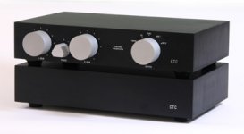
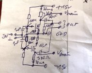
Here in the middle my version. Slightly less beautiful and refined, I know…. But still trying to keep up with the original design! (To a loving father, every child looks most beautiful ;-))
It has the same 5 position input, but only one volume control (with LDRs), and the phase switch has a middle “zero” position that serves as output mute.
(Trying to structure everything into individual posts, based on the topic)
Here in the middle my version. Slightly less beautiful and refined, I know…. But still trying to keep up with the original design! (To a loving father, every child looks most beautiful ;-))
It has the same 5 position input, but only one volume control (with LDRs), and the phase switch has a middle “zero” position that serves as output mute.
Attachments
The case is made from two aluminum sheets (top and bottom), held by side plates made from wood, and the front- and backplates also from aluminum. All metal sheets are 4mm thickness. Here is a picture showing the structure of the case.
Another picture shows how the top plate is recessed, by the thickness of the heatsinks mounted on top, to achieve a flat top surface. The heatsinks are SK105 from Fischer-Elektronik, with 15mm thickness.
Another picture shows how the top plate is recessed, by the thickness of the heatsinks mounted on top, to achieve a flat top surface. The heatsinks are SK105 from Fischer-Elektronik, with 15mm thickness.
Attachments

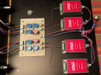
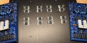
The whole thing is powered with switchmode DCDC converters (+/- 48V and +/-12V, independent for both channels), and the input voltage is a 24V SMPS, hence no second case for the PSU. Attached are the pictures showing the power supplies.
On the right side, four DCDC converters take the input 24V to create the +/-48V for the amplifier. On the perfboard are some post-filters to reduce high frequency noise, and additional DCDC converters to convert the input 24V to +/-12V for the relays and servos.
They are all mounted to the bottom side of the case, to provide the necessary cooling. In operation they hardly heat up, so no problem there.
Attachments
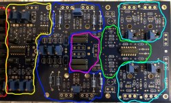
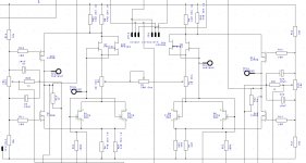
Here a picture of the (partly stuffed) PCB I made (one per channel), indicating the different functional blocks.
Turns out the PCB was designed with a rather hot needle, so it looked quite different once I had finished debugging ;-)
(Sorry, I don’t think I will make these PCBs available, since the bug fixing part would be very frustrating to everybody – believe me I’ve been there ;-( )
Red (on the left): Input selection reed relays
Yellow: LDR-based attenuator
Blue: The actual amplifier circuit
Purple: Output phase selection
Green: Servo
Blue-green: Voltage regulators
Attachments
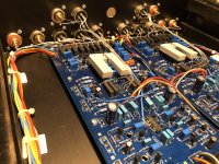
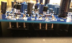
This shows the amplifier PCBs in the case, along with the input / output wiring and all the control leads for the relays and volume. The well-trained DIY eye will easily spot the additional cables, resistors, modifications, …. Took me quite some time to iron everything out…..
Attachments
But what is that grey blob on top of the amplifier stage? It's a 3D printed heat spreader.... I wanted to put something to protect the JFETs from temperature differences, a simple copper foil would have done but we live in the 21st century, so I opted for something more rocket-sciency ;-)
The material I wanted is ceramics, but that would have been crazy expensive, so I settled for aluminum-filled nylon. Put some thermal grease on top of the transistors, and carefully slide it over them, fix with a screw.
The material I wanted is ceramics, but that would have been crazy expensive, so I settled for aluminum-filled nylon. Put some thermal grease on top of the transistors, and carefully slide it over them, fix with a screw.
Attachments
The power transistors (Fairchild FQA19N20 / FQA12P20) are mounted below the PCB. The second picture shows the “sandwich”, and the mounting screw is accessible through a hole in the PCB. I actually had enough space in the amplifier, but this was more of a challenge ;-)
The transistors are first mounted onto the metal plate with silicone pads, screws not fully tight. Then, the PCB is lowered onto the transistors and each lead of the eight transistors carefully inserted, then the PCB is fixed with some screws and distance pieces, finally the transistor mounting screws are tightened and then the solder joints made. That ensures least possible mechanical stress on the solder connections.
The transistors are first mounted onto the metal plate with silicone pads, screws not fully tight. Then, the PCB is lowered onto the transistors and each lead of the eight transistors carefully inserted, then the PCB is fixed with some screws and distance pieces, finally the transistor mounting screws are tightened and then the solder joints made. That ensures least possible mechanical stress on the solder connections.
Attachments
And, just as a side comment – I have never before built a line stage with 15dB gain, using 16 power transistors in TO247 package... ;-)))
The MOSFETs were also matched, using a little test circuit sketched on the back of an envelope (literally ;-)), a little amplifier with the same bias current as in the final amplifier, with 0.5V RMS sinus input, measuring the output amplitude, and matching the transistors for output amplitude as close as possible, both N and P. Of course, the gate voltage needs to be adjusted, for every transistor to run at identical drain current.
Attachments

The circuit itself has been exhaustively explained in this thread, by the man himself: John Curl's Blowtorch preamplifier
… and I certainly haven't added any wisdom to this simple, elegant and very well performing circuit.
It is a difference amplifier with complementary JFETs, current-mirrored (kind of...) into output stages with MOSFETs in grounded gate configuration. Hope that description is correct ;-)
The JFETs used here are 2x PF5102 (n-ch) and 2x J270 (p-ch) per branch. I had a bunch, and measured them all for threshold voltage and transconductance, using a Peak Atlas DCA75, and finally settled for this combination. Simulation was indicating that of the PF5102 would be ok to handle 2x J270, but in the real circuit that was not so, I ended up with a constant negative offset, that was finally cured by adding another n-ch.
The trimpots between the source pins were planned to adjust for distortion, the middle one for gain, but in the end it turned out that my measurement options were not up to the task, so I left them in the middle and only adjusted the gain between the two stereo channels.
The outer trimpots were used to adjust the DC offset on the outputs to as close to zero as possible. This took a lot of going back and forth, since there was some thermal drifting going on, with the amplifier settling in at the right bias points, so I needed about one hour or so to get it done. (The servo was not connected for this exercise, it was only hooked up afterwards, so I could adjust to the “native” bias point, and hope the servo would keep it there, its influence being really weak....)
Attachments
Here is the schematic of the servos. The signal is picked up from the outputs, and the control signal is fed back into the trimpots used for initial offset correction. I used ye olde TL074, to make a 3rd order lowpass filter and then amplify a little bit before feeding the control signal back in. It follows the rule of “make the servo so weak that it doesnt regulate any more, and then back up just a little”. Resulting output offset is below 1mV (essentially the opamp input offset), very stable.
Attachments
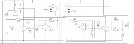
The attenuator is also located on the PCB, based on LDRs. I used NSL-32 and they work like a charm! The whole “lightspeed attenuator” threads were very inspiring to me, and I had a long-standing itch to build one of those....
The picture only shows one divider = half of the attenuator, since the whole amplifier is fully symmetric. The circuit I developed is a little over the top.... It contains voltage-controlled current sources, made with ¼ of a TL074 each, driving a bipolar transistor to set the current in each LED. The input voltage is a DC voltage coming from the (stereo) volume pot, lowpass filtered and buffered.
Each current source can be adjusted in level and also in current gain, with two independent trimpots, as I was thinking the LDRs might differ in both absolute value as well as slope. But alas, that did not seem to be the case here, so I ended up adjusting the current identical in all four current sources for max level, and then only played with the “level” to adjust the attenuation.
Interesting phenomenon, while adjusting the different currents in the LEDs (with a fixed input voltage connected to all four inputs – L/R of both channels all parallel) , there was a lot of drifting, associated with individual heating of the LEDs and maybe also the LDRs. I had to go back and forth several times for each setting. First, I started with full volume and adjusted all level trimpots so that identical AC voltage was measured at each input. Then, I repeated the process for multiple settings of the volume pot (50%, 25%, 75%, and several other values). It did not matter so much which exact value the volume pot had, I basically adjusted away all the differences between the two channels including the volume pot itself. The whole process, with thermal settling in between each change, probably took me 5-6 hours... But the result is worth it – less than 1% deviation across the entire volume range, down to something like 5% or so...
Attachments
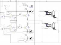
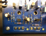
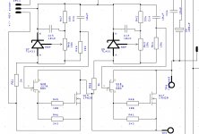
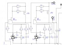
The supply voltage to the amplifier stage is +/- 24V. It is made out of +/- 48V input voltage via two cap follower stages, that both have a stabilized input, so they are not exactly pure cap followers.....
The pictures show the positive and negative regulators separately. In all four, there is a “cell” that consists of a TL431 with a trimpot to adjust the voltage, and a JFET/MOSFET combo to follow that voltage. In between the TL431 and the JFET gate is a little lowpass filter to remove noise introduced by the TL431 or the input rails.
The first stage brings the voltage down to 34V (noting that the TL431 max voltage is 36V, a close shave ;-)) and the second stage then to 24V.
Attachments
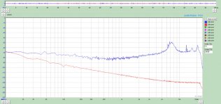
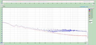
But, how good are these regulators? Here is a picture of the supply rail noise on the incoming 48V after the DCDC converter, with my DMM I could measure a few mV AC voltage on that rail but there is an ugly bump at 7kHz. (Measurements were done with a rail noise probe – basically, a large capacitor to block the DC, fed into my external soundcard Steinberg UR22 with 24bit resolution, the red signal is the other channel of the interface, connected to ground).
Attachments
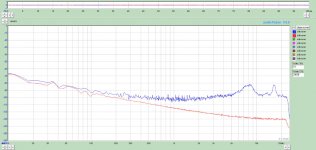
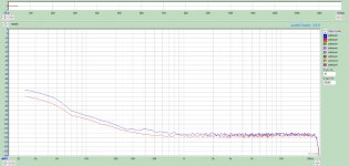
Unfortunately, this amplifier clearly exceeds my measurement capabilities, so I have just a few pictures to illustrate a little bit what is possible. The picture shows the output with volume set to zero, and -10dB represent 0.14V (RMS). With Noise down at -115dB, from this I figure the SNR to be -120dBmW (referenced to 0.775V RMS, that means). When connected to the power amplifier, with no signal and volume fully up, hardly any noise can be heard.
Attachments
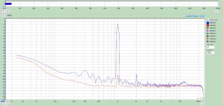
This picture shows the output of the amplifier with volume set to roughly 60% , and output voltage 0.14V RMS, fed by a ultra low distortion sine oscillator. The oscillator has K2 at -88dB, K3 at -102dB, and no more. Built through a group buy on diyaudio.com, after an application note from Linear Technology.
This amplifier has K2 at -87dB compared to the input signal, 1dB worse. And K3 sits at -100dB, similar to the oscillator.
So, I am not sure to be able to measure this amplifier as it would be needed. Guessing better power supply, a more noise free room, and an isolated measurement box would be needed to improve – my poor kitchen table won't do.
Attachments
- Home
- Source & Line
- Analog Line Level
- My private blowtorch clone