These are really impressive numbers that you are achieving! We really need to see a loop-gain plot!
See here for a good guide:
https://sites.google.com/site/frankwiedmann/loopgain
Simpler tasks (apologies if some of these don't make sense from a circuit operation, as opposed to optimisation, point of view; I have not had a chance to study your circuit or description of operation):
Referring to the component references from the schematic in post #79:
What happens to the THD numbers if you: remove Q16? If you change the Q19/Q22 current source to a two-transistor negative-feedback current source?
Both of these changes reduce component count so I'm interested to see what differences they make.
Also R7 and R8 look very small. Noise performance improves if these are larger. Can they be made larger (e.g. up to 330R) without upsetting circuit operation?
Sadly, the 2SA1407 & 2SC3601 are no longer manufactured 😕

If you purchase some you will have to verify through measurement that they are genuine parts.
You could try something like the KSA1381/KSC3503 aka 2SA1381/2SC3503 pair. Only the "K" prefix is still manufactured (by Fairchild).
See here for a good guide:
https://sites.google.com/site/frankwiedmann/loopgain
Simpler tasks (apologies if some of these don't make sense from a circuit operation, as opposed to optimisation, point of view; I have not had a chance to study your circuit or description of operation):
Referring to the component references from the schematic in post #79:
What happens to the THD numbers if you: remove Q16? If you change the Q19/Q22 current source to a two-transistor negative-feedback current source?
Both of these changes reduce component count so I'm interested to see what differences they make.
Also R7 and R8 look very small. Noise performance improves if these are larger. Can they be made larger (e.g. up to 330R) without upsetting circuit operation?
Sadly, the 2SA1407 & 2SC3601 are no longer manufactured 😕
If you purchase some you will have to verify through measurement that they are genuine parts.
You could try something like the KSA1381/KSC3503 aka 2SA1381/2SC3503 pair. Only the "K" prefix is still manufactured (by Fairchild).
Hi Harry,
Thanks for commenting 🙂 I've tried a few of your suggestions. Removing Q16 worsened THD by only 0.000005%. I also tried with an input cascode in the past but that didn't seem to bring improvement so I left it out. R7 and R8 could be increased without impact; no change to THD. I haven't tried yet a different CCS though.
Meanwhile I made a scaled up version that does 250/8, 500/4.
Here's the THD for a 500W 20K sine 😀
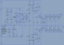
The schematic uses 4 output pairs (though these really need to be 200V types) and a double buffer.
I read the link on loop gain and noticed that LTspice comes with an example too. I'll look at it and apply it to my circuit and see what it comes up with 🙂
As for those drivers, that's really a bummer they're no longer made. I'll see if I can find models for the ones you suggested.
Thanks for commenting 🙂 I've tried a few of your suggestions. Removing Q16 worsened THD by only 0.000005%. I also tried with an input cascode in the past but that didn't seem to bring improvement so I left it out. R7 and R8 could be increased without impact; no change to THD. I haven't tried yet a different CCS though.
Meanwhile I made a scaled up version that does 250/8, 500/4.
Here's the THD for a 500W 20K sine 😀
Code:
[SIZE=2]
Fourier components of V(out)
DC component:-0.0172544
Harmonic Frequency Fourier Normalized Phase Normalized
Number [Hz] Component Component [degree] Phase [deg]
1 2.000e+04 6.360e+01 1.000e+00 179.58° 0.00°
2 4.000e+04 3.519e-06 5.532e-08 169.01° -10.56°
3 6.000e+04 1.993e-05 3.134e-07 -49.91° -229.48°
4 8.000e+04 2.612e-05 4.107e-07 -157.56° -337.14°
5 1.000e+05 1.406e-05 2.210e-07 116.35° -63.22°
6 1.200e+05 7.248e-06 1.140e-07 -150.60° -330.17°
7 1.400e+05 6.777e-06 1.066e-07 -58.32° -237.89°
8 1.600e+05 1.187e-05 1.867e-07 -145.01° -324.59°
9 1.800e+05 5.698e-06 8.959e-08 -53.57° -233.15°
10 2.000e+05 9.579e-06 1.506e-07 -140.61° -320.18°
Total Harmonic Distortion: 0.000064%
[/SIZE]I read the link on loop gain and noticed that LTspice comes with an example too. I'll look at it and apply it to my circuit and see what it comes up with 🙂
As for those drivers, that's really a bummer they're no longer made. I'll see if I can find models for the ones you suggested.
Attachments
Starting to have fun 🙂
I'm VERY (period) unexperienced using LTspice, so probably I did not do everything in the right way. Anyway, I changed the input trannies to be my favourite Dual JFET, adjusted R7/8 and built an OPS based on a massive load of OnSemi's (again massive) BJTs and increased the rails a little (in a real world design I'd probably go for a shuntie for VAS and also the +-15V would get a more clever reg 😉).
From what I was able to sim the 20k output looks real good, though I dunno how to measure THD etc. I attached a plot as well as the asc, just in case someone would like to play or comment.
 View attachment 5BJT.asc
Next step I'd like to try is to reduce BJT count to 3 (should still be stable on 4R loads) and to introduce distributed drivers, something I really love to play with.
Thank you so much for providing such a nice playground! 😀
BR,
Holgi
I'm VERY (period) unexperienced using LTspice, so probably I did not do everything in the right way. Anyway, I changed the input trannies to be my favourite Dual JFET, adjusted R7/8 and built an OPS based on a massive load of OnSemi's (again massive) BJTs and increased the rails a little (in a real world design I'd probably go for a shuntie for VAS and also the +-15V would get a more clever reg 😉).
From what I was able to sim the 20k output looks real good, though I dunno how to measure THD etc. I attached a plot as well as the asc, just in case someone would like to play or comment.
View attachment 5BJT.ascNext step I'd like to try is to reduce BJT count to 3 (should still be stable on 4R loads) and to introduce distributed drivers, something I really love to play with.
Thank you so much for providing such a nice playground! 😀
BR,
Holgi
It looks like you included the parameters and directives too so the THD is already measured for you on each .tran run. Just hit CTRL+L to view the error log, that's where the THD results are written to.
It's fun trying different output stages and power levels; now we have base THD values with an ideal OPS, it becomes fairly easy to see differences.
Meanwhile I'm trying to get the loop gain. I have to duplicate the circuit for that hah.
It's fun trying different output stages and power levels; now we have base THD values with an ideal OPS, it becomes fairly easy to see differences.
Meanwhile I'm trying to get the loop gain. I have to duplicate the circuit for that hah.
I have to duplicate the circuit for that hah.
Study the link I provided earlier. Circuit duplication is not necessary and the sims can be done with a simple stepping process instead. Having said that, it is usually easier to have two entirely separate schematic files: one for loop-gain sims and another for transient simulations.
Hm, I already had a look into the err log, no word about fourier there 😕
Did I miss a checkbox somewhere?
Did I miss a checkbox somewhere?
I see you have two .tran directives, one from my schematic and a separate one. You'll have to uncomment or delete the one on the left. A THD output is added only when you do a transient analysis, not an ac analysis.
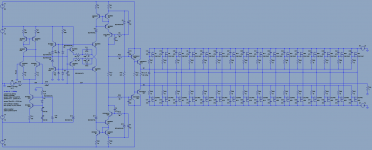
Meanwhile I thought: Let's get crazy and load up that VAS already. So here the previous schematic with the quadruple amount of output devices for a 2000W into 1 ohms. I had to slow down the buffer slightly to make it stable again. It's still sub-ppm. Don't laugh at the rows of trannies 😛
[/SIZE]
Meanwhile I thought: Let's get crazy and load up that VAS already. So here the previous schematic with the quadruple amount of output devices for a 2000W into 1 ohms. I had to slow down the buffer slightly to make it stable again. It's still sub-ppm. Don't laugh at the rows of trannies 😛
Code:
[SIZE=2]
Fourier components of V(out)
DC component:-0.0172533
Harmonic Frequency Fourier Normalized Phase Normalized
Number [Hz] Component Component [degree] Phase [deg]
1 2.000e+04 6.360e+01 1.000e+00 179.57° 0.00°
2 4.000e+04 5.303e-06 8.338e-08 170.21° -9.37°
3 6.000e+04 3.586e-05 5.638e-07 -52.97° -232.54°
4 8.000e+04 3.740e-05 5.881e-07 -155.81° -335.38°
5 1.000e+05 1.859e-05 2.922e-07 119.25° -60.33°
6 1.200e+05 1.037e-05 1.631e-07 -150.30° -329.87°
7 1.400e+05 9.722e-06 1.529e-07 -56.09° -235.66°
8 1.600e+05 1.704e-05 2.679e-07 -142.60° -322.17°
9 1.800e+05 8.752e-06 1.376e-07 -53.62° -233.19°
10 2.000e+05 1.378e-05 2.166e-07 -138.14° -317.71°
Total Harmonic Distortion: 0.000097%Attachments
Sorry guys, I'm still struggling a little with LTspice. I've now implemented example LoopGain2.asc and added the function to my plot.defs file.
But the question is, how do I plot it? Do I use the function name in the 'Add Trace' dialog?
But the question is, how do I plot it? Do I use the function name in the 'Add Trace' dialog?
This level of speed is easy to achieve in SPICE without adding parasitics to the Mfets. The difficulty is to make it stable at all output voltages and currents. See my posts here:
http://www.diyaudio.com/forums/soli...ign-attempt-number-2-simpler.html#post3539618
And here:
http://www.diyaudio.com/forums/solid-state/171159-bob-cordells-power-amplifier-book.html#post3540588
http://www.diyaudio.com/forums/soli...ign-attempt-number-2-simpler.html#post3539618
And here:
http://www.diyaudio.com/forums/solid-state/171159-bob-cordells-power-amplifier-book.html#post3540588
This level of speed is easy to achieve in SPICE without adding parasitics to the Mfets. The difficulty is to make it stable at all output voltages and currents. See my posts here:
http://www.diyaudio.com/forums/soli...ign-attempt-number-2-simpler.html#post3539618
And here:
http://www.diyaudio.com/forums/solid-state/171159-bob-cordells-power-amplifier-book.html#post3540588
Indeed. MagicBox, see also post #3638 in the second thread linked to above for another way to predict trace inductance.
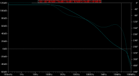
On your loop gain plots, please could you turn off phase unwrapping? If you do this, there will be a discontinuity in the phase plot at ±180 degrees, making it easier to see phase and gain margins.
Talking of which, yours are scarily low. You need to make the unity loop gain frequency lower in order to increase your margins.
Now that you can do the loop gain plot, you can try doing it at different operating points. For example, you can try different DC operating points by AC-coupling the load with a large capacitor (e.g. 1 kF) and then adding some DC bias to the input signal. This will adjust the DC-voltage operating points of the circuit without also increasing the output current. You can also test at different current levels by adding an ideal current source from the output to ground.
Last edited:
@keantoken
You mean the 47pF caps right? Well, they don't do much in the sim but on a real OPS this capacitance was enough to silence a local 80MHz oscillation in the Exicon output devices. Though this was in conjunction with low gate resistors. So, I wouldn't call them parasitics, rather, stabilizers. On the other hand, I could probably increase the gate stoppers.
I now put the KSC3503/KSA1381 drivers in. Sadly enough they worsened THD a bit, about 50% worse but still acceptable 🙂 A quick look on Mouser told me these are the best I can get without having to hunt old stock.
I think it's time to make a PCB for the 200W/4Ohm;100W/8Ohm prototype version. I'll update the schematic one more time to reflect this version.
By parasitics I mean trace inductance. 1 inch of inductance can have a surprising effect. According to Cordell, each Mfet has 5nH gate and drain inductance, and 13nH source inductance, before the pins even leave the case. External inductances will probably be larger.
I also played around a little. Modifications:

Will play a little more with various level/freq sims tomorrow and also start a PCB layout if and when everything looks fine 😀
- 3 BJT pairs with distributed drivers
- Simple regulators for +-15V input stage supply (+-68V for VAS to be powered by good low-noise reg)
- Offset and Bias adjust added
Will play a little more with various level/freq sims tomorrow and also start a PCB layout if and when everything looks fine 😀
By parasitics I mean trace inductance. 1 inch of inductance can have a surprising effect. According to Cordell, each Mfet has 5nH gate and drain inductance, and 13nH source inductance, before the pins even leave the case. External inductances will probably be larger.
Ah okay 🙂 Yeah I haven't taken the time yet to begin adding parasitics. IRF lists the lead inductances in the datasheet for their hexfets. I'm affraid it's going to be a lot of work to model the most significant parasitics.
Meanwhile I've tried to improve the gain and phase margin, but the only way I can succeed in that is by increasing the IPS emitter degens. This makes the OLG drop and THD increase severely. I wonder if I can remove the phase dip around 1MHz in a different manner.
Well, in my first link are some symbols I created which make inserting trace inductances much more convenient. Convenience is key, really. Sometimes you have to design your own tools.
Holgi, one of the advantages to distributed driver is that you can use faster devices like the C3503/A1381. I've read many other people saying they don't like the MJE150xx pairs even for non-distributed drivers because of their enormous parasitic capacitance. Using them this way you seem to be multiplying the problem you are trying to fix.
Holgi, one of the advantages to distributed driver is that you can use faster devices like the C3503/A1381. I've read many other people saying they don't like the MJE150xx pairs even for non-distributed drivers because of their enormous parasitic capacitance. Using them this way you seem to be multiplying the problem you are trying to fix.
Holgi, one of the advantages to distributed driver is that you can use faster devices like the C3503/A1381. I've read many other people saying they don't like the MJE150xx pairs even for non-distributed drivers because of their enormous parasitic capacitance. Using them this way you seem to be multiplying the problem you are trying to fix.
Thanks keantoken, I came around this playing with higher input freq, you probably cannot compensate the MJEs in my setup. Will try your suggestion 🙂
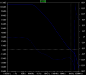
Here a new OLG plot. I've been able to create around 60 degrees phase margin, a gain of 40 degrees compared to the OLG plot atop this page 🙂 Unfortunately I had to sacrifice THD for it.
The changes were an increase of the LTP degens a big deal, and a snubber network.
The changes were an increase of the LTP degens a big deal, and a snubber network.
Attachments

- Status
- Not open for further replies.
- Home
- Amplifiers
- Solid State
- My New VAS Topology