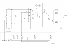
Here's one more thing I stumbled upon with the simulation. Please have a look at the schematic.
I've included the parasitic resistance and inductance of some idealized PCB tracks, the absolute values are not that important. I've also included a run of the inevitable speaker wire. The big quesion is: Where do I put the stimulus? If I put it "on the PCB", so to say (point "B"), I get pretty much the same results that Tom got. Layout makes a huge difference here, see the red and green traces "B" for comparison.
If I include the speaker wire though and put the stimulus directly at the load (point "A"), the differences in layout routing get mostly swamped by the speaker wire. Compare red and green traces "A". The result looks rather bad in both cases, so there's not much to be gained with careful routing.
Which way is the correct one? And why?
Anything wrong with the placement of the measuring VCVS? IMHO it is correctly placed always directly across the load. If not - why not?
The green traces show the "layout" like it is shown in the attached schematic. All Grounds are connected to a ground star, which itself is connected to the power source, except for the signal ground, which is connected directly to the speaker return. The red traces show basically the same layout, but now with all the grounds connected to the ground star (like how I did it on the boards). "A" and "B" respectively depict where the stimulus was connected to.
Attachments

Are the A plots where you applied the stimulus across the load, R1?
Whereas the B plots have the stimulus applied from the top of the load (R1) to point B at the other end of the speaker cable?
What does it look like when the stimulus is applied from out to B, i.e. at the start of the speaker cable?
Whereas the B plots have the stimulus applied from the top of the load (R1) to point B at the other end of the speaker cable?
What does it look like when the stimulus is applied from out to B, i.e. at the start of the speaker cable?
Must admit I never understood the real benefit of routing the signal ground to the output terminal, since this only results in fabulous measurements right at the o/p terminal.
This is is efffectively remote sensing of the ground (via the ground end of R11), which seems a bit irrelevant if you are only correcting for an inch or two of track and then you have a few metres of wire that is outside the correction loop.
This is is efffectively remote sensing of the ground (via the ground end of R11), which seems a bit irrelevant if you are only correcting for an inch or two of track and then you have a few metres of wire that is outside the correction loop.
Whereas the B plots have the stimulus applied from the top of the load (R1) to point B at the other end of the speaker cable?
No. The A plots have the stimulus (I1) connected from point A to "simulator ground", like is seen in the schematic. The B plots have it connected from point B to sim ground instead; "left" from the speaker wire so to say. Points A and B are both on the negative side of the load and thus the stimulus is not connected across the load.
This is is efffectively remote sensing of the ground (via the ground end of R11), which seems a bit irrelevant if you are only correcting for an inch or two of track and then you have a few metres of wire that is outside the correction loop.
That's exactly what I think the sim is telling me here...
Do you mean between A and the junction between V2 and V3 ?No. The A plots have the stimulus (I1) connected from point A to "simulator ground", like is seen in the schematic. The B plots have it connected from point B to sim ground instead; "left" from the speaker wire so to say. Points A and B are both on the negative side of the load and thus the stimulus is not connected across the load..............
and between B and the junction between V2 and V3?
What are these measuring?
Yes. V2 and V3 are the power supply, +-30VDC. Quite like the smoothing caps on a real PCB in this case.
In the simulation, the inputs to the amplifier are grounded to GND_SIG and an AC current is injected into the GND_LOAD net. This represents the current returning from the speaker load. The return current results in an error voltage developing across the ground nets, part of which is amplified by the LM3886. The simulation uses a voltage controlled voltage source (VCVS) with a gain of 1 V/V to measure the resulting error voltage developed across the load. The resulting error voltage is plotted in dBV. Recall, the goal here is to have as little error voltage developed across the load as possible, as this error will degrade the THD performance of the amplifier.
LM3886 chip amp grounding.
what is your sim measuring?
explain what the graph scales mean?
explain what the graph scales mean?
Really? 😕
In the simulation, the inputs to the amplifier are grounded to GND_SIG and an AC current is injected into the GND_LOAD net. This represents the current returning from the speaker load. The return current results in an error voltage developing across the ground nets, part of which is amplified by the LM3886. The simulation uses a voltage controlled voltage source (VCVS) with a gain of 1 V/V to measure the resulting error voltage developed across the load. The resulting error voltage is plotted in dBV. Recall, the goal here is to have as little error voltage developed across the load as possible, as this error will degrade the THD performance of the amplifier.
That's one. The other is frequency range, pretty self-explanatory. Not sure what you're after... 😕
Usually an argument. ....
My argument is, that the routing of the speaker return track becomes more or less negligible if you consider the parasitics of the inevitable speaker wire - unless you build an active speaker, of course. In my opinion those couple of inches are merely a short extension of the speaker wire and thus the speaker wire as a whole must be considered in the simulation. Tom did not model the speaker wire in his simulations at all. I resembled his sim from the pictures seen on his website, changed the circuit topology to the MyRef, and added some parasitics for the speaker wire.
Now I was not sure where to put the stimulus there, because I didn't come up with the sim, but merely copied it. There were basically two options, which I called A and B. In B the results are pretty much the same as Tom's, which seems reasonable, because the load itself and the speaker wire are "out of the loop". In A however, the current of the stimulus now has to pass through the speaker wire and the PCB track, which makes the results a lot worse to begin with. Now the routing of the track makes only a difference of a couple dB, compared to 80+dB in B.
I'm not 100% certain which way is right, though. That's why I posted the results here after all. But then again, in my opinion, the speaker IS the signal generator, because the current has to pass through it and anything induced by back-EMF originates there, so the stimulus has to be placed directly at the load itself.
Andrews questions sounded to ME like he was questioning the simulations itself, and not asking for an argument. "What is the sim measuring / explain the graph scales" sound to me like he didn't understand what the sim is supposed to show. That's why I linked to Tom's original article and quoted the most relevant part, because HE explains HIS simulations there in depth. Since I merely copied/adapted/redid his technique, I thought it would be more than adequate to link to his original work and at the same time give him credit where it is due.
I apologize for any misconceptions this has caused and hope my point is more clear now.
OK, I think most of us are agreed, I'm thick.
I don't understand what the simulator is telling me.
I don't know the question you have asked of it and I don't know what the answer to that question is telling me.
I don't understand what the simulator is telling me.
I don't know the question you have asked of it and I don't know what the answer to that question is telling me.
The simulation shows you the voltage between the speaker return (point A in the schematic) and the non-inverting input of the amplifier circuit, which is basically at signal ground. This voltage results from the 1A stimulus current and the parasitic resistance/inductance of the speaker wire and the PCB tracks between those points. Since this error voltage is seen by the amp input, it gets amplified and added to the output signal. At least that's how I understand it. Maybe Tom can chime in and enlighten us all.
My argument is, that the routing of the speaker return track becomes more or less negligible if you consider the parasitics of the inevitable speaker wire - unless you build an active speaker, of course. In my opinion those couple of inches are merely a short extension of the speaker wire and thus the speaker wire as a whole must be considered in the simulation.
Spot on!
Taking this a step further...
Remote sensing of the speaker wire will reduce distortion at the speaker terminals, the downside is that it's much trickier to keep the loop stable.
Or the other way round - moving the sensing point away from the amp o/p teminal to "nearer" the LM3886 will worsen distortion at the amp o/p but help with transient response and stability. More phase margin means you can extend the loop gain out a bit higher whuch gives lower distortion etc etc
It all about tradeoffs.
Last edited:
I'm starting to understand that.
Can I look at the other end of your stimulus input.
Why is there an idealised PSU with zero impedance feeding the four voltage outputs?
Why have you shown the Signal Ground separate from the injection point?
Why is the "star ground" not used as the injection point.
I don't see how applying the impulse to the idealised PSU is replicating a real amplifier.
Why is there an idealised PSU with zero impedance feeding the four voltage outputs?
Doesn't make a difference in AC simulation to use a more elaborate PSU model.
Why have you shown the Signal Ground separate from the injection point?
Because in a physical build there is a lossy trace between those points, whose parasitics are modeled with resistance and inductance.
Why is the "star ground" not used as the injection point.
Because the injection point, IMHO, is the connector at the cabinet of the speaker. This can not be the star ground, because there's the speaker wire in between. If, on the other hand, the injection point and all the other grounds are connected to a single star ground (only possible in the sim), you get an ideal result far below -200dB, which surely not resembles reality.
I don't see how applying the impulse to the idealised PSU is replicating a real amplifier.
The PSU is not important here. And the sim is not supposed to replicate a real amplifier. It is only supposed to show how an error voltage due to the load current develops and gets amplified by the amp. This alone could be achieved with a much simpler simulation schematic I guess, but then again the sim should somehow resemble the actual circuit AND PCB layout.
Take all of this with a grain of salt, because this is all just how I understand it and I don't claim to fully understand it myself.
😱
Are you familiar with LTspice? I'll post the sim file when I'm back home, then you can give it a try for yourself.
Are you familiar with LTspice? I'll post the sim file when I'm back home, then you can give it a try for yourself.
- Home
- Amplifiers
- Chip Amps
- My new monobloc layout for Mauro Penasa's MyRef Rev. C