Note that you shouldn't overdo things with high-value bias resistors either - the LM4562 family (including LME49720) may not start up reliably in some (especially single supply) scenarios then. Seems that their internal bias current cancellation circuitry needs a while to start up, and until then non-negligible bias current needs to be supplied externally. That shouldn't be an issue for you though.
BTW: What kind of supply voltages have you been thinking of? It's recommended not to go above +/-18 V since things do get rather warm at this point, and +/-12..15 may be a better idea. 17 such OPs will need about 150-160 mA.
Speaking of power, you'll need to adhere to power amplifier layouting guidelines (separate signal and power grounds, low-inductance rail etc.).
Thanks for your thoughts. I haven't posted the updated schematic yet, but for the LME I dropped the (+) input to ground resistor to 22k.
I was planning on using +/- 15V PS boards that use 317/337 regulators with a capacitor added to the adjust pin to reduce noise. The regulators are heatsink mounted and should easily meet the current needs. Even with operating currents and output currents considered its only a few hundred mA in total.
Yes, as you mentioned some details about the layout must be considered.
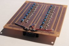
I've started doing some assembly. I've soldered in all the IC sockets, put 0.1uF bypass caps between the power supply pins of each, a 10uF cap on each rail to ground, the terminal block for power connections, and some power distribution leads.
.
.
Attachments
I made some more progress but I am now a little unsure of the best way to proceed...
I need to run several "busses". There is one to supply the input to all the amplifiers in the output stage for each channel (left+right), plus another pair to carry the output current away to the 'phones. I decided that the best way to run the "output" busses is to bridge over to another identical proto PCB from each output trace via the output isolation resistor. I can then easily collect the outputs onto one of the bus strips of the PCB, and can keep the outputs away from the rest of the circuit.
For the inputs, I could run a wire around the top (bare) side of the proto board that is connected to the output of the drive amplifier (the first op amp). I would then run wires up from the input traces on the circuit side of the board to the top side, and solder them to the input bus there. That would help to keep inputs and outputs separated. But the wire would just be hanging out there.
Should I be concerned with noise + hum pickup for a wire not near a ground in this circuit, or is this not a big deal?
Hi Charlie
How is the build going?
Just bought a huge load of NE5532 from Avnet for a steal and got some wirewound output resistors to isolate the opamps but am going a lot lower in resistance. 1.3R I think Self used 1R on the opamplifier. I have some .33uf rifa films for the rails and found a great source for cheap proto quantity pcbs. I have contemplated this style amp for years. Then saw the Maier photo about five or six years ago and new it would work but never got around to it. Now forcing myself to try it. Hoping to learn from your experiments before I order boards.
Uriah
active feedback for lower distortion
Here is a suggestion to consider. Since the NE5532 are duals, use 1/2 of each op-amp in the feedback loop as active feedback to reduce distortion from the lower harmonics as discussed here
http://www.diyaudio.com/forums/solid-state/26600-lowering-buffer-opamp-distortion.html
with the circuit picture in post #3. It would require twice as many op amps but what the heck, they are cheap. Using the other half of each op amp in the feedback loop is preferable to using a separate op amp in the loop, as discussed in the thread, since the other half experiences the same package heating as the half that is being loaded.
Last edited:
Here is a suggestion to consider. Since the NE5532 are duals, use 1/2 of each op-amp in the feedback loop as active feedback to reduce distortion from the lower harmonics as discussed here
http://www.diyaudio.com/forums/solid-state/26600-lowering-buffer-opamp-distortion.html
with the circuit picture in post #3. It would require twice as many op amps but what the heck, they are cheap. Using the other half of each op amp in the feedback loop is preferable to using a separate op amp in the loop, as discussed in the thread, since the other half experiences the same package heating as the half that is being loaded.
No need for overkill... this design should have very, very low THD as is.
Hi Charlie
How is the build going?
Just bought a huge load of NE5532 from Avnet for a steal and got some wirewound output resistors to isolate the opamps but am going a lot lower in resistance. 1.3R I think Self used 1R on the opamplifier. I have some .33uf rifa films for the rails and found a great source for cheap proto quantity pcbs. I have contemplated this style amp for years. Then saw the Maier photo about five or six years ago and new it would work but never got around to it. Now forcing myself to try it. Hoping to learn from your experiments before I order boards.
Uriah
I stopped to figure out how I will wire up the input and output buses. I have more or less figured that out, however, I need to do some intricate soldering because I need to attach wires to places that are partially blocked by existing components. I've been working on other stuff that is more pressing...
This project is still something that I intend to finish, but I have had to re-prioritize my efforts on some other stuff. I hope to get back to this project at the end of OCT. I may design a PCB for the project and give up trying to wire so many devices point-to-point, as that has been challenging!
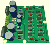
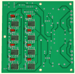
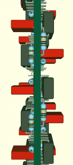
I found a break in the action to do some more design work on my headphone amplifier. I decided to abandon the proto board and instead design and fab a proper PCB for the amp and on-board power supply. I'm using the same 101x101mm footprint that I have used for other projects.
The AC supply uses independent dual secondaries. These feed two rectifiers and are followed by CRC filtering, which lead to LM317/LM337 regulators. I used star grounding, with separate stars for the regulated ground and main PS filtering caps. Although the stars must be are connected, this should help to keep the regulated ground quiet. According to one of my references, this physical arrangement keeps the rectifier current pulses from circulating through the ground, which reduces rectifier noise. The CRC arrangement should help this as well. The regulators will be connected by a bracket to a low profile heatsink that will make up the top of the chassis.
When initially laying out the amplifiers on the available board area I could not fit all the 5532 packages that I intended to use. There are 32 amplifiers in parallel per channel, so that's 32 DIP-8 packages in total. I also wanted to have on-board power regulated supplies. Constrained by the small amount of space, I had to get creative!
Using my design software, Target 3001!, I Was able to come up with a novel way to tightly pack the 5532s: alternating the placement of the DIP packages between the top and bottom of the board. Also, where there was a DIP package on one side, in that same PCB real estate but on the opposite side I could locate the bypass cap for the op-amp as well as a resistor, if needed. This also made it possible to orientate adjacent packages so that their pins were identical, e.g. pin1 of one DIP package was next to pin 1 of the next DIP package, pin2 next to pin2, and so on. As a result I could place these pins right next to each other. As I began to build up the layout, symmetries appeared that made it possible to pack everything in to the limited space very efficiently.
I have to say that the "3D View" feature of Target 3001! came in very handy during this whole process. It generates a 3D mockup of the board that you can pan and rotate to look at various parts of the board as it will look when its been fabricated. This helped me find several misplaced labels and get some feel for the placement and routing that the 2D layout does not provide. Screen shots taken from the 3D view of the board are attached, below.
There a view of the top of the board, one of the bottom, and a "side" view to highlight the placement of parts on both sides of the board.
I sent the design to the fab and it should be back here in a week or so.
Attachments

I've been working on the same thing Charlie except that I'm using a few hundred and surface mount. Its modular so I'll be trying it out as a headphone amp and power amp. In regards to trying to get creative you might find that with efficient layout you can get away with one cap per two opamps per rail. Also (you may already be doing this) Self was using one cap across the rails between two opamp packages. The cool thing was that if it crosses the rails between two opamp packages then it can go from pin 7 on one to pin 4 in the other. Traces are then single digit mm long.
across the rails doesn't help much unless you have bridged/floating load
with SE gnded load all the load current returns through the gnd and that is where the local PS caps should terminate to reduce loop area
with SE gnded load all the load current returns through the gnd and that is where the local PS caps should terminate to reduce loop area
A few hundred... wow. What rail voltages are you planning to use? I think that you will find that to be the limiting factor when used as a power amp... And how are you planning to get the heat out? If you can increase the density using the SMD version you can probably use one cap per two packages (maybe between them?) and it will still be "close enough". IIRC less than a 2-3 cm is fine.
I am using the cap between PS rails and in my layout I can place components (like this cap) under the IC package directly, making the tracks from PS pin to cap to PS pin very short. On the other hand, the PS rail tracks between the output caps of the regulators and the 5532s is rather long. Hopefully this will be a non-issue. That's why you prototype!
I am using the cap between PS rails and in my layout I can place components (like this cap) under the IC package directly, making the tracks from PS pin to cap to PS pin very short. On the other hand, the PS rail tracks between the output caps of the regulators and the 5532s is rather long. Hopefully this will be a non-issue. That's why you prototype!
Last edited:
across the rails doesn't help much unless you have bridged/floating load
with SE gnded load all the load current returns through the gnd and that is where the local PS caps should terminate to reduce loop area
Tell that to Douglas Self...
read his book more carefully - he had a point that he was making at the time, gives other advice - to improve the gnd in another place in the same book
regulated supply makes a difference in his argument too
clever people without deep subject knowledge often get stuck on isolated statements without understanding the full context
with 3 decades of analog design experience in Industrial/Scientific Instrumentation including Av 8000 strain gage amplifiers inches from 100 MHz DSP/CPU/Ethernet/USB I can put these issues in proper context
I am confident in my domain knowledge, comfortable (rarely) "correcting" Doug Self
particularly when it just a matter of interpretation/context
read his book more carefully - he had a point that he was making at the time, gives other advice - to improve the gnd in another place in the same book
regulated supply makes a difference in his argument too
clever people without deep subject knowledge often get stuck on isolated statements without understanding the full context
with 3 decades of analog design experience in Industrial/Scientific Instrumentation including Av 8000 strain gage amplifiers inches from 100 MHz DSP/CPU/Ethernet/USB I can put these issues in proper context
I am confident in my domain knowledge, comfortable (rarely) "correcting" Doug Self
particularly when it just a matter of interpretation/context
I think that we are talking about two different things... I think. I was talking about using 0.1uF bypassing caps between the rails at the IC. Of course there are also large electrolytic caps of a few 1000's of uF from each rail to ground that support the load current.
Which "book" are you referring to? He has published several. Giving that kind of very non-specific advice "go off and do some reading" is not helpful.
I got a smoking deal on nearly 2000 ne5532. So im going for ridiculously low output impedance. I dont think heat will be an issue but ill keep an eye on it and make adjustments if necessary.
I will try both SE and BAL. BAL for power amp for sure. I'll try adjustable supplies starting with 15v rails and increase.
JCX I read more in the book and know what you are talking about. Power input to each module will have a small sea of caps for the return on SE.
I'm just working on board design right now so looking forward to your results Charlie.
Oh, additionally the ne5532 modules will be working as a buffer. The gain circuit will be on a separate board so I can try different front ends.
local high frequency bypass should be to gnd too - >99% of op amp's develop Vgain by a (single polarity) rail referenced stage - that rail really wants to be well bypassed to the signal reference gnd for PSRR, high frequency stability
rail-to-rail typically only helps with the op amp internal AC current demand - so can be useful - but not by itself
some discussion around fig 7 http://www.analog.com/static/imported-files/application_notes/AN-202.pdf with a (old) list of op amps integrating stage reverence supply terminal
rail-to-rail typically only helps with the op amp internal AC current demand - so can be useful - but not by itself
some discussion around fig 7 http://www.analog.com/static/imported-files/application_notes/AN-202.pdf with a (old) list of op amps integrating stage reverence supply terminal
Last edited:
local high frequency bypass should be to gnd too - >99% of op amp's develop Vgain by a (single polarity) rail referenced stage - that rail really wants to be well bypassed to the signal reference gnd for PSRR, high frequency stability
rail-to-rail typically only helps with the op amp internal AC current demand - so can be useful - but not by itself
some discussion around fig 7 http://www.analog.com/static/imported-files/application_notes/AN-202.pdf with a (old) list of op amps integrating stage reverence supply terminal
This link, in a related thread, has a quote from Douglas Self on the 5532 rail-to-rail bypass caps:
http://www.diyaudio.com/forums/anal...e-return-current-flow-pcbs-6.html#post4070160
This is the blueprint that I have used in this project for bypass cap usage.
- Home
- Amplifiers
- Headphone Systems
- My LM5532 Headphone Amplifier project