Hi Russ:
Quick and excellent answer, for the lazy among us 😀
Well, I''ll have to find the time to mod it 😉
Pitty, I liked that big MKP10 input cap
Best regards
Mauricio
Quick and excellent answer, for the lazy among us 😀
Well, I''ll have to find the time to mod it 😉
Pitty, I liked that big MKP10 input cap
Best regards
Mauricio
what goes here?
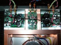
As you can see I am in the process of populating the boards and was wondering what components go in the areas identified below...
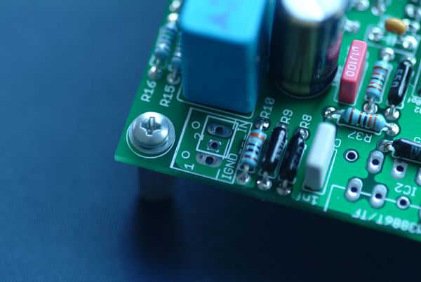
IGND - - ?
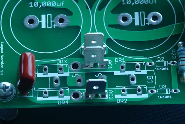
DR1 DR2 DR3
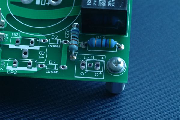
LED Light emiting diode i assume, does one of the white connectors go in here with a lead out to the front of the case if i wish?
mark
As you can see I am in the process of populating the boards and was wondering what components go in the areas identified below...
IGND - - ?
DR1 DR2 DR3
LED Light emiting diode i assume, does one of the white connectors go in here with a lead out to the front of the case if i wish?
mark
Hi Mark,
I think I see what you are asking... I will take a stab.
Top picture - Input header, or terminal block with input GND and input. Use either not both.
Middle picture - rectifier bridge or four MUR diodes. Use either not both.
Bottom picture - Power indicator LED header or terminal block. Use either not both.
Cheers!
Russ
Hi Russ,
Thanks, I did not fully appreciate the bridge rectifier options, but it is obvious now that you mention it,of course the MUR option would be different.
With regard to the top photo, the first solder pad (nearest the edge) is input ground, the next one immediatley to it's right is also input ground but is there for if you use the connector arrangement - and the next one on the right is input.
My apologies if this has been covered through the thread but to look back over nearly 300 pages is a little daunting...
Mark
D1GGY said:Hi Russ,
With regard to the top photo, the first solder pad (nearest the edge) is input ground, the next one immediatley to it's right is also input ground but is there for if you use the connector arrangement - and the next one on the right is input.
My apologies if this has been covered through the thread but to look back over nearly 300 pages is a little daunting...
Mark
You have it correct. The left two are IN_GND in the right pad is IN_HOT.
No worries. 🙂

Cheers!
Russ
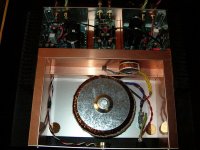
Do you mean measure? Or do you mean take to another circuit?
You can measure the voltage between the two large capacitors. You could also take it to another circuit from there is you had a mind to.
Cheers!
Russ
You can measure the voltage between the two large capacitors. You could also take it to another circuit from there is you had a mind to.
Cheers!
Russ
Pics of input and led options
An externally hosted image should be here but it was not working when we last tested it.
An externally hosted image should be here but it was not working when we last tested it.
Yes I've to bring them to an other circuit.
So I bring them from the two big caps.
Thanks
Andrea
So I bring them from the two big caps.
Thanks
Andrea
Another option.
I usually measure of the input side of the 1K dropping resistors that feed the zener supply. You get the 34 -35 volts on one side and 12 on the other. It also works as a good pick off.
George
I usually measure of the input side of the 1K dropping resistors that feed the zener supply. You get the 34 -35 volts on one side and 12 on the other. It also works as a good pick off.
George
Yeh 😉 Strange idea.
But computers are so small now that I thought why I
couldn't add it as a signal source for RevC amplifier
and put everything into one box 🙂
There are lots of HTPC (home theatre PC) projects why
we couldn't make audio PC 🙂
Actually audio part occupies about 70-80% of the box.
The rest is for computer which doesn't generate any
audible noise because it has fanless motherboard and
there is no hard drive (Linux loads from USB flash memory).
Loseless audio files (FLAC) it loads through Wi-Fi from
another computer taking out transport from this equation 🙂
The only noise comes through EM emmitance from the
motherboard and I think it's in the whole range - audible
and above. I'm trying to protect audio part from that noise
as much as possible.
Wow!! That is Sawwwweeeeeeet! I like how you partitioned the trafo/amp/kook. Very well thought out layout man. 
How did it work out?
Cheers!
Russ
How did it work out?
Cheers!
Russ
Re: Another option.
Hi George,
do you mean R1 and R4?
Where I exactly get +34/35, -34/35 and 0?
Thank you and sorry but I wouldn't fried up the PCB...
Andrew
Panelhead said:I usually measure of the input side of the 1K dropping resistors that feed the zener supply. You get the 34 -35 volts on one side and 12 on the other. It also works as a good pick off.
George
Hi George,
do you mean R1 and R4?
Where I exactly get +34/35, -34/35 and 0?
Thank you and sorry but I wouldn't fried up the PCB...
Andrew
Can someone post a summary of all documents needed, it's impossible for me to read all 230+ pages and find the right documents.
Maybe a little tip for the thread starter, to keep a summary in the first post of the latest info required to build one.
I have very limited electronics knowledge, building something from a schematic, and recognizing the different parts isn't a problem. But i don't have enough knowledge to understand why things are connected the way they are, thats also part of the problem why i can't find the right set of documents i guess. When " I " build one, i let someone do it with more skills, but having all the required documentation would be essential 😉
I already got the my_ref_rev3.pdf document 🙂
Thanks in advance 🙂
- Home
- Amplifiers
- Chip Amps
- My "audiophile" LM3886 approach