If I were to use all that power, I would definitely render myself deaf like a stone. There are 500W of continuous power with flat frequency response. It is not a matter of how powerful the speakers are, but more a quest of building an amplifier that can use all the potential of the power stages and power supply that I already have. At home, unless one is endowed with a huge mansion, one cannot use big audio powers, as that encroaches on other people's freedom to enjoy their property in peace.
At an impedance of 8 Ohm, and a power of 250W continuous, using P = V^2/(2R) where V is the peak voltage.
Substituting we get:
250 = V^2/(2*8)
=> 250*2*8 = V^2
=> V = [250*2*8]^(1/2)
=> V = 63 volts approx.
Since the power supply is a mammoth that can deliver a power that sustains 1500W of audio power continuously, I need to find a way to efficiently derive a much lower voltage, +/-30V, to drive my amplifier at home. One way is to partially unwind the secondaries and make a tap midway each half coil. That way the voltage would be halved. However, this procedure requires me to have proper transformet tape available that is not very easy to get in my location. A two pole two way mechanical switch would switch between full voltage and the much reduced voltage for indoor home use.
Post Scriptum:
Oddly enough, I found that if I remove the current mirror from the amplifier I posted and replace it with two resistors and a diode, the distortion figure would be reduced to 0.03%. The differential pair's current would still remain balanced. I am attaching the circuit. The voltage reduction mechanisms are not shown.
Attachments
If I were to use all that power, I would definitely render myself deaf like a stone. There are 500W of continuous power with flat frequency response. It is not a matter of how powerful the speakers are, but more a quest of building an amplifier that can use all the potential of the power stages and power supply that I already have. At home, unless one is endowed with a huge mansion, one cannot use big audio powers, as that encroaches on other people's freedom to enjoy their property in peace.
At an impedance of 8 Ohm, and a power of 250W continuous, using P = V^2/(2R) where V is the peak voltage.
Substituting we get:
250 = V^2/(2*8)
=> 250*2*8 = V^2
=> V = [250*2*8]^(1/2)
=> V = 63 volts approx.
Since the power supply is a mammoth that can deliver a power that sustains 1500W of audio power continuously, I need to find a way to efficiently derive a much lower voltage, +/-30V, to drive my amplifier at home. One way is to partially unwind the secondaries and make a tap midway each half coil. That way the voltage would be halved. However, this procedure requires me to have proper transformet tape available that is not very easy to get in my location. A two pole two way mechanical switch would switch between full voltage and the much reduced voltage for indoor home use.
Post Scriptum:
Oddly enough, I found that if I remove the current mirror from the amplifier I posted and replace it with two resistors and a diode, the distortion figure would be reduced to 0.03%. The differential pair's current would still remain balanced. I am attaching the circuit. The voltage reduction mechanisms are not shown.
This is the .asc file. I mistakenly attached the wrong schematic. This should be with the current mirror removed and the constant current source feeding the differential pair input replaced by a series pass regulator. As said the distortion figure improved by a factor of 3.
Attachments
It seems basically OK, at least in simulation although I'm wondering whether you should include some base stopper resistors on the multiple output pairs.
What is a base stopper resistor? I tried google to understand the theory behind it, but I couldn't find anything apart from various schematics that are always difficult to understand without the proper foundations.It seems basically OK, at least in simulation although I'm wondering whether you should include some base stopper resistors on the multiple output pairs.
The output stage including the driver stage was taken from a public address amplifier (Wharfedale S1500). Therefore, I am assuming it is professionally designed and does not need any tweeking. As I wrote in other threads and probably also in this one, the original amplifier had a very weird grounding scheme with the hot output terminal connected to the common terminal. I am attributing the amplifier's failure to its grounding scheme although I am not 100% confident of this. With the hot output terminal connected to ground, the input would find itself oscillating at the output voltage. I find the latter as bad design and that is why I am attributing the amplifier's failure to its grounding scheme.
Base stoppers have long been used to increase stability when multiple pairs are in use. Bob Cordell elaborates on this a little in his book and goes on to say that they counter the reducing impedance vs frequency as seen by the base. The effects of stray L and C components (board and layout) can be negated by base resistors... all things that can work against stability. Such problems can also be very device dependent and modern high power transistors generally have a much more extended transition frequency and far less gain droop than older types. All these are things that can work to our advantage but also they are things that demand care in use and implementation.
You might really be reaching a point where you need to knock up a prototype in order to explore possible problems that are not showing up in the simulation.
You also almost certainly need some form of output inductor in series with the load. If you add a 1uF cap across the output you will find it oscillates. That might seem a crazy test, but its valid and one that should not upset the amplifier.
You might find these interesting (generally). Andrew has posted regularly on here in the past.
http://hifisonix.com/wordpress/wp-content/uploads/2011/03/The_e-Amp_V2.03.pdf
Power Amplifiers
And on grounding:
Ground Loops: How to Wire-up an Audio Amplifier for Zero Hum and Noise
With a voltage of +/-85V the risk of component damage is great, therefore, I am planning to use wirewound series resistors to limit the power supplies current. If the amplifier works as it should, the voltage drop across the resistors should be low, if not, something would certainly be wrong.You might really be reaching a point where you need to knock up a prototype in order to explore possible problems that are not showing up in the simulation.
The output stage already has such an inductor but I have bypassed it when I built a low voltage prototype. The inductor is connected on the 0V rail instead of the hot power output terminal, so I have to do some desoldering without damaging the output stage to place the inductor on the hot output terminal.You also almost certainly need some form of output inductor in series with the load. If you add a 1uF cap across the output you will find it oscillates. That might seem a crazy test, but its valid and one that should not upset the amplifier.
I am curious how an inductor, something that naturally likes ringing, can actually prevent the output from oscillating. Probably, the inductor prevents oscillations by forcing the output current to be more in phase with the input. A capacitor on the output certainly prevents the output current from being in phase with the voltage.
I will check the output current phase if it is considerably displaced from that of the output voltage.
P.S.
I checked the phase but found the current and voltage are actually in phase. So, the oscillations are caused by something I do not yet understand.
Last edited:
Although your rails are high, that doesn't stop you using a DBT (bulb tester) in series with the transformer primary. Your bias currents are low and so the amp should come up to almost full voltage if all is well.
The rising impedance vs frequency of the inductor serves to isolate the amplifier output from any capacitive loading, whether deliberate for testing or just high capacitance cables (which can upset some amplifiers that don't have such an inductance. Naim was a well known casualty many years ago). Electrostatic speakers are another tough load that can approximate to a capacitor loading.
The inductor must always be air spaced, never one with a magnetic core. Somewhere around 5uH would be typical for most designs.
The original 2 micro-Henries inductor is a ferrite rod with very thick wire wound around it. It is a short ferrite rod with several turns of wire. So, a big part of the magnetic circuit is through air, which has a very high reluctance. I assume, the designers at Wharfedale, did take care that the core never saturates under designated load conditions.
I copied both the series RC and parallel LR circuits and added them to the output. Now, with a capacitance of 1 micro-Farad across the load does not cause any oscillations.
I also added base resistors at the driver stage. I am attaching the resultant circuit.
P.S.
Thank for the simple, yet brilliant idea of using a light bulb in series with the primary of the amplifier. This is an inexpensive method, yet effective and safe.
Attachments
Last edited:
Most (but not all) amplifiers of this type would need a Zobel network connected directly from the output to ground (in other words connected before the inductor). That's pretty standard across the board really.
Adding another R/C circuit on the output side is sometimes done to help prevent RF ingress back into the amplifier caused by long speaker leads.
Remember that while testing with squarewaves is a great tool for exploring stability, they bear little relation to real world audio signals. Any nicely damped ringing you see at the speaker output when squarewave testing into capacitive loads is just the result of the inductor doing its job and not problem with the main amplifier.
Interesting 🙂
There is a little bit here on practical implementation of twin Zobel networks based on around the LM3886 chip.
LM3886 Chip Amp Stability Analysis
Base stoppers... the driver ones are fine but I was actually meaning to add them to each power output transistor. They would be low in value, perhaps in the 2.7 to 3.9 ohm region.
The original circuit did not use base stoppers for the output power transistors, and since I want to keep the power stage, I cannot use such resistors. I tried to move the Zobel RC series network before the inductor and the distortion figure rose a little bit, so I lowered the capacitance, and if my memory serves me right, the distortion figure improved a little bit.
I am inspecting the various currents in the circuit and found horrible looking artifact currents at frequencies from 2MHz to 8MHz. Although the output was a sine wave, I am worried that such artifactual currents are undesirable for any serious amplifier design. I also reverted back to using a current mirror and constant current source in the input stage. To filter off current artifacts, I used two 2200 Ohm resistors in series with a capacitor in parallel the series resistors. I am attaching the modified circuit which now also has a buffer stage between the VAS and driver stage. The distortion figure for a 16kHz signal is around 0.05%.
Theres is still some residue of artifactual currents.
Attachments
The preceding circuit failed the square wave test with heavy ringing. The frequency response chart, Vout VS Frequecy, has a weird shape. At about 100KHz it rises to a maximum above the low frequency plateau, then it steadily drops almost to zero at about 200kHz.

To properly amplify a square wave signal, an amplifier must have an infinite frequency response. This is the theory based in Mathematics. A square wave with a fundamental of 20kHz cannot be properly amplified with an audio amplifier that is sensitive to only its fifth harmonic. Since I tested a square wave signal at 20kHz, I was bound to get heavy ringing due to the amplifier's limited frequency response. In fact, a square wave of 1000Hz was reproduced far better than the one at 20000Hz. The only 'artifacts' were a substantial overshoot and undershoot. The latter two are to be expected, at least in my inexpert opinion, since there is an inductance on the output line.
The current artifacts seem to have been reduced considerably although there are still some oscillations. I do not think it is good to use critical damping as that would impact heavily on the slew rate.
This is my inexpert opinion.
The current artifacts seem to have been reduced considerably although there are still some oscillations. I do not think it is good to use critical damping as that would impact heavily on the slew rate.
This is my inexpert opinion.
Have a look at post #157 and the following posts here:
My MOSFET amplifier designed for music.
which show squarewave testing of my own amplifier from 1kHz upwards.
Post #161 details the bandwidth of the amp.
Different thread, different ideas:
New Design-HEXFET Poweramp. Sonic benefits of this approach.
My MOSFET amplifier designed for music.
which show squarewave testing of my own amplifier from 1kHz upwards.
Post #161 details the bandwidth of the amp.
Different thread, different ideas:
New Design-HEXFET Poweramp. Sonic benefits of this approach.
The attachment shows a square wave test with my latest version of the circuit. There is ringing at both edges of the square wave. I am posting, and I beg pardon if I am being a nuisance, as I do not know whether this amount of ringing is normal.
Attachments
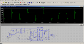
Its perfectly normal because it is the inductance and load capacitance alone that is causing the ringing. I think you will find the voltage at the input to the inductor looks much cleaner.
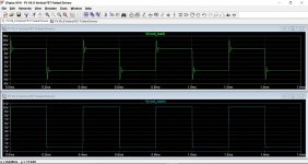
This shows a design of mine with the output voltage shown before and after the inductor.
Also try this. You will see the source voltage is always a perfect squarewave but the load voltage rings... how much depends on the values of the components and load.
This shows a design of mine with the output voltage shown before and after the inductor.
Also try this. You will see the source voltage is always a perfect squarewave but the load voltage rings... how much depends on the values of the components and load.
Attachments
With a raw gain of 50 (not dB), the distortion figure went down to 0.026% for an output of 16.5V peak. This was simulated for a 20000kHz signal.
Let us check what happens to the distortion figure for a 1kHz signal. For the same signal output, the distortion is at 0.001278%. The load is 8 Ohms, which means a power of:
P = V^2/(2R) (V is peak voltage)
P = 16.5^2/(2*8)
P = 17W
Notwithstanding the latter is a mouth watering distortion figure, I will continue with my quest of getting similar or better distortion figures for more power.
Attachments
- Home
- Amplifiers
- Solid State
- My attempts at a design of a 3 stage amplifier