The amplifier channel that is laid next to the toroidal transformer has the biggest hum problem. The other one may have it, but it is barely audible. Removing the input connections from the channel with the hum does not resolve it. This means, flux leakage from the toroidal transformer is generating hum voltages in the input stage of the affected channel.
I am trying to find a way of using a magnetic shield between the transformer and the affected PCB.
I am trying to find a way of using a magnetic shield between the transformer and the affected PCB.
You will probably need to have a transformer manufacturer fit a copper strap around your toroid. You should also twist the transformer secondary wires.
Is the hum 50Hz (smooth and deep sound) or 100Hz (rough, buzzing sound)? That will guide you as to what the source of hum is; whether mains borne (primary winding and wiring) or rectified secondary wiring.
Looking at the layout of boards, I see the input wiring is fairly close to the R channel power supply so I would shield the input sockets and wiring with a thin piece of sheet steel which was earthed to the chassis.
If it hasn't already been suggested, experts recommended that the power transformer is rotated until there is minimal hum. The strongest radiation comes from the leads at the point where they exit the toroid - a good reason not to trim leads back before checking this out or perhaps locating the lead exit point furthest from sensitive low level signal areas.
My persistent posts to this thread may indicate I am not satisfied with this amplifier. Trying it with large loudspeakers (250W continuous, 1000W intermittent) was very satisfying for me. The sound is good and the power enough to force me to keep the volume controls to 20% of maximum for fear of damaging my hearing. The volume potentiometers are linear and are from the original circuit.
I am very thankful for this forum and for the nice experts who helped me through this project. The hum issue is another small challenge, that I am embracing to learn more, notwithstanding I am not a youth, and now almost 52 years old.
I was assuming flux due to free current carrying conductors was negligible, but I was wrong. Rotating the transformer is also a very easy to do idea.
Thanks for everyone's patience.
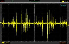
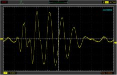
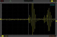
The oscilloscope is USB type model Hantek 6074BC.
Testing is pointing in the direction of amplifier self oscillation. The supply ripple seems to be triggering this behaviour as the audible sound is like a 50Hz mains hum.
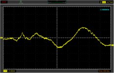
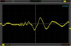
I am attaching various images of the scope's window at different time bases. The patterns continously change although the jpg images are static. I am also attaching the scope's image with the amplifier turned off. The output isolating and coupling component is a 3cm ferrite ring with 8 or 9 turns as primary and secondary. The high noise level with the amplifier turned off may be explained by the ferrite toroid picking stray radio signals.
Post Sciptum:
It seems logical to me to re-simulate the amplifier circuit complete with the power supply. The latter should include the transformer, rectifier and smoothing capacitors.
I am very thankful for this forum and for the nice experts who helped me through this project. The hum issue is another small challenge, that I am embracing to learn more, notwithstanding I am not a youth, and now almost 52 years old.
I was assuming flux due to free current carrying conductors was negligible, but I was wrong. Rotating the transformer is also a very easy to do idea.
Thanks for everyone's patience.
The oscilloscope is USB type model Hantek 6074BC.
Testing is pointing in the direction of amplifier self oscillation. The supply ripple seems to be triggering this behaviour as the audible sound is like a 50Hz mains hum.
I am attaching various images of the scope's window at different time bases. The patterns continously change although the jpg images are static. I am also attaching the scope's image with the amplifier turned off. The output isolating and coupling component is a 3cm ferrite ring with 8 or 9 turns as primary and secondary. The high noise level with the amplifier turned off may be explained by the ferrite toroid picking stray radio signals.
Post Sciptum:
It seems logical to me to re-simulate the amplifier circuit complete with the power supply. The latter should include the transformer, rectifier and smoothing capacitors.
Attachments
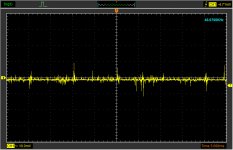

Toroids are very immune to pick up, you may be seeing the wiring pickup between amp and toroid when the amp is off. Yes there's a strong resonance there around 1MHz.
But this might be the toroid inductance resonating with the scope input capacitance - its normal to just use x10 probe direct to the output
But this might be the toroid inductance resonating with the scope input capacitance - its normal to just use x10 probe direct to the output
The amp may be oscillating with the ferrite, 8 turns on a suppression toroid is a near short at audio frequencies. Just use a x10 probe at the speaker output.
If it hasn't already been suggested, experts recommended that the power transformer is rotated until there is minimal hum. The strongest radiation comes from the leads at the point where they exit the toroid - a good reason not to trim leads back before checking this out or perhaps locating the lead exit point furthest from sensitive low level signal areas.
Thanks for that little gem, Ian.
Such a simple test to try out when trying to fight hum.
Its hard to say for sure without actually being able to see how it all behaves. Yes, the amp output should be clean although it can be 'normal' to see all kinds of noise on the incoming supply that is superimposed on the 50/60Hz sine.
That's not much help I know 🙁
You could try loading the rails (bulbs ?) to see if the increase in ripple alters the amplifier output.
That's not much help I know 🙁
You could try loading the rails (bulbs ?) to see if the increase in ripple alters the amplifier output.
Recalling the amplifier circuit there are two points where interference from the mains can enter the signal path. These are the current sources' bias diode chain and the input cascode's bias Zener diode. If my memory serves me right, avalanche is a noisy process, which implies noise from avalanche is being fed into the signal path, albeit it is largely suppressed by the cascode's output impedance. With this injection, the signal is very slightly soiled with all random types of interference from the mains. The same thing happens at the current sources' bias point.
I will simulate further to investigate what I wrote above.
Post Scriptum:
The VAS's current source's current is modulated by the ripple voltage according to LTSpice. The modulation follows the ripple waveform. This is in agreement with a much simpler prototype circuit that I built before this amplifier. Connecting an electrolytic capacitor across the prototype's bias diodes greatly reduced the ripple.
Instead of two rail bulbs I connected a bulb in series with the mains toroidal transformer. The hum became very weak if not obliterated altogether.Mooly said:You could try loading the rails (bulbs ?) to see if the increase in ripple alters the amplifier output.
There are two inputs to your amplifier. One of these has a capacitor of 2200uF connected between the inverting input and earth. Physically this would have to be relatively large.
Instead of two rail bulbs I connected a bulb in series with the mains toroidal transformer. The hum became very weak if not obliterated altogether.
I was meaning the bulbs as a load on the rails this time... to draw current and increase ripple.
I am pointing my fingers at the current sources' bias voltage. This is from a dropper resistor and two series connected signal diodes. The latter have very quick response times, which means, the bias voltage is not stable as it should be. LTSpice shows that there is a 9mV variation with a supply ripple of 5V peak-to-peak. This has the effect of varying the VAS's standing current and also the differential input standing current. My logic tells me, that if the variation in standing currents is not such that its effects by the input on the VAS and vice versa, do not completely cancel out, a ripple voltage should appear at the output. The reason is, any increase in current by the input stage into the base of the VAS amplifying transistor, should be such, that it is exactly the amount required to cancel the effect in the VAS.
Last edited:
CCS circuit blocks have good power supply rejection. If you look at your positive supply rail you have the Vas emitter connected directly to this without any RC decoupling of the rail to earth.
That means any ripple on the positive supply is going to compromise your Vas as the carriers in transistors originate from the collector and most of these sweep past the base to the collector (of the carrier charges).
The same applies to the diode string although with three in series these will not pass any current unless the base of the Vas is lower than the voltage drop through the three series diodes. You should run your simulation and pick the visible traces tool and check VN020.
Thanks for all your replies and patience.
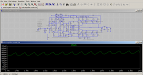
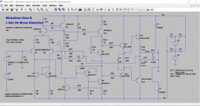
I am back using LTSpice to simulate for power supply ripple and mains interference effects on the output of the amplifier. Thanks to whoever developed LTSpice these effects are being captured which means I am not in the dark. Mjona suggest decoupling the +ve rail with an an RC network at the VAS's amplifying transistor, but I cannot figure out how this is done. The current sources' bias chain has been modified to use two 10k series resistors with the centre point connected to a 1uF capacitor whose other terminal is connected to the negative rail. With this I am getting a 3mV complex ripple at the output. The ripple voltage is a 5V sawtooth waveform on both rails. This means, a ripple of 10V peak to peak is being simulated from rail to rail.
I would like to simulate random voltage transients on the power mains. Any suggestions as to how this is done are most welcome.
Thanks for all your replies and patience.
I am back using LTSpice to simulate for power supply ripple and mains interference effects on the output of the amplifier. Thanks to whoever developed LTSpice these effects are being captured which means I am not in the dark. Mjona suggest decoupling the +ve rail with an an RC network at the VAS's amplifying transistor, but I cannot figure out how this is done.
In the attached file which has a NPN Vas the RC network R35/C15 in the negative supply rail. The output stage switching action generates a spray of transients on the supply rails so some means of isolating the small signal stages from the output stage is necessary - especially so with a high power amplifier where the effects are greater in scale.
Attachments
Thank you so much. This is much much better than before. Using 20*log(psu_ripple/output_ripple) I got 100dB! If this formula is the right one, the amplifier is exhibiting a power supply rejection of 100dB.
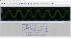
I am attaching a screenshot of ltspice while simulating this.
I am attaching a screenshot of ltspice while simulating this.
Attachments
That looks better. The spray of harmonics I mentioned occurs when switching on half cycles radiates in the ether. Another example of this is a car ignition coil without any suppression. A neighbour somewhere close by has a lawn mower that interferes with TV reception. You should consider the other two suggestions I made in relation to the toroidal transformer.
Have a look at this with the power supply set up as a 'real' AC supply.
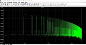
The amp is running at close to maximum output and the reservoir caps are just 2200uF in order to generate lots of ripple.
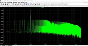
If we look at the FFT of the output we can see the ripple component superimposed on the amplifier output.
You could also load the rails with a resistor to introduce ripple and then look at the amplifier output with no signal applied. That is the last image and the rail ripple is almost 10 volts pk/pk per rail (20 ohm loading on each).
Simulating like this assumes perfect grounding which of course the real amp will not (can not) ever match.
The amp is running at close to maximum output and the reservoir caps are just 2200uF in order to generate lots of ripple.
If we look at the FFT of the output we can see the ripple component superimposed on the amplifier output.
You could also load the rails with a resistor to introduce ripple and then look at the amplifier output with no signal applied. That is the last image and the rail ripple is almost 10 volts pk/pk per rail (20 ohm loading on each).
Simulating like this assumes perfect grounding which of course the real amp will not (can not) ever match.
Attachments
- Home
- Amplifiers
- Solid State
- My attempts at a design of a 3 stage amplifier