Stefanoo said:
When you meant to say that the circuit is nothing special, you meant to say that there are better topologies that can be used? if so, would you like to give any suggestion?
I have to agree with Paul here. If you look at the high end Japanese phono circuits from the eighties you will see a lot of similar designs. No idea what Paul's suggestion for a better topology would be but i would suggest another look at the Vendetta.
analog_sa said:
I have to agree with Paul here. If you look at the high end Japanese phono circuits from the eighties you will see a lot of similar designs. No idea what Paul's suggestion for a better topology would be but i would suggest another look at the Vendetta.
Hi Analog,
I have looked at vendetta sch.
It is a nice design but:
1) i would like to do something different
2) i prefer not to use Servo controls
Said that, Vendetta is definitely an high end design but i would like to work this out first.
You said that many japanese designs are like mine and i am sure it is...but....i tried to reasearch some infos on balanced VAS stages but i couldn't find anything useful.
May you post a schematic and/or a link for these type on designs?
This would definitely help to track down the problem!
Stefanoo,
my pleasure.
IRF610 and IRF9610 are badly matched, IRF9610 has different, poorer characteristics, even IRF610 is significantly nonlinear.
Biasing this way, the unstable Vgs is excluded and lower Vref used.
Good luck in your efforts.
my pleasure.
IRF610 and IRF9610 are badly matched, IRF9610 has different, poorer characteristics, even IRF610 is significantly nonlinear.
Biasing this way, the unstable Vgs is excluded and lower Vref used.
Good luck in your efforts.
Analog,
thank you.
This is helpful.
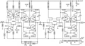
My configuration is different although i use a balance VAS like this.
Plus, my MC stage is made with cascode common source Jfets.
I can see on this circuit that there is a split RIAA as well.
The circuit is made of two identical blocks.
Lets just analyze the first one:
First stage is a differential amplifier cascoded with a passive load (i am wondering if an active load would work on that position but as paul hypotized active mirror load works for SE config).
Second stage the Balance VAS stage, cascoded(bootstrapped?!..man i still don't catch the bootstrap config), no current mirror.
Anyways on the VAS stage: is the output (2SC959) a simple common emitter follower config (?!) with low output impedance, is it right?
I mean on my configuration i had the cascoded mirror with current source active load and a resistor to bias the push-pull class A output stage.
interesting thing is that compensation capacitors are asymmetrical and are way ower than the usual standard 100pF used on the SE Vas version, which it is great, which means faster response and less load on the front end for the charging and unchargin compensation cap's job.
I have noticed the power supply is to low voltage value, why?
I mean...i have noticed that my circuit started to oscillate if the voltage was increased....but i didn't have compensation caps.
The VDs of the devices is properly set at around 7V.
No output coupling CAP need nor compensation DC cap on the negative feedback to latch unity DC gain, since the monolithics and the bla config contribuites to a very low DC drifting.
It's a good circuit.
I just don't like the output stage though.
thank you.
This is helpful.
My configuration is different although i use a balance VAS like this.
Plus, my MC stage is made with cascode common source Jfets.
I can see on this circuit that there is a split RIAA as well.
The circuit is made of two identical blocks.
Lets just analyze the first one:
First stage is a differential amplifier cascoded with a passive load (i am wondering if an active load would work on that position but as paul hypotized active mirror load works for SE config).
Second stage the Balance VAS stage, cascoded(bootstrapped?!..man i still don't catch the bootstrap config), no current mirror.
Anyways on the VAS stage: is the output (2SC959) a simple common emitter follower config (?!) with low output impedance, is it right?
I mean on my configuration i had the cascoded mirror with current source active load and a resistor to bias the push-pull class A output stage.
interesting thing is that compensation capacitors are asymmetrical and are way ower than the usual standard 100pF used on the SE Vas version, which it is great, which means faster response and less load on the front end for the charging and unchargin compensation cap's job.
I have noticed the power supply is to low voltage value, why?
I mean...i have noticed that my circuit started to oscillate if the voltage was increased....but i didn't have compensation caps.
The VDs of the devices is properly set at around 7V.
No output coupling CAP need nor compensation DC cap on the negative feedback to latch unity DC gain, since the monolithics and the bla config contribuites to a very low DC drifting.
It's a good circuit.
I just don't like the output stage though.
Hi Stefano, I built a 250W mosfet amplifier with a differential VAS like this over 20 years ago, so I don't need to build another to prove it works! When I say the circuit is not special, I mean that the basic architecture is well established. John Linsley Hood covers VAS balanced architectures in his Valve and Transistor amplifiers book, and shows how to progressively inprove their performance.Stefanoo said:
Hi paul,
When you meant to say that the circuit is nothing special, you meant to say that there are better topologies that can be used? if so, would you like to give any suggestion?
any advice is of course very welcome.
Why not start simple, and get familiar with the basics of feedback compensation before adding cascodes, and current mirrors which just make the job more complex. Have you tried the mimimalistic approach, as in Nelson Pass designs, which are REALLY low feedback if that is your thing!
analog_sa said:Hi Stefano
Not sure if this is what you are looking for but there are several interesting circuits by Kaneda.
If the schematic you posted is supposed to be a phono stage (it certainly looks like one) then, from a noise perspective, it is hard to imagine a worse design.
thank you syn 🙂
i mean...i trie it out on a BREADBOARD and i didn't have noise issue although the circuit wasn't inside any enclosure, no ground plane....nothing..and the only slight noise was due to main 50Hz.
I don't think that noise is the most important thing on phono design...just my two cents.
Anyways, if you mean to say that Jfets don't suit for good low noise designs, you will find me partailly in agreement.
If you drive the input with low impedance source, then you are likely going to have not the best noise performance on the air.
The only way to get around this is to parallel transconductance matched devices.
A bach of 4 lowers noise a lot.
In my design i went for the maximum number of parallel jfet to still keep the HF stability which is 6.
IMO the second stage is a differential Jfet amp which doesn't have noise issue due to the fact that the cascoded common source paralleled jfet AC coupled has high output impedance and therefore jfets are going to be lower noise than BJTs.
if you have any suestions i will be glad to take it into consideration.
Thank you for your post.
syn08 said:
If the schematic you posted is supposed to be a phono stage (it certainly looks like one) then, from a noise perspective, it is hard to imagine a worse design.
Not sure what the exact background is but looking at the 560k input resistor i would assume this circuit works with a step-up transformer. Never claimed it was excellent for noise or in any other respect.
paul joyce said:
Hi Stefano, I built a 250W mosfet amplifier with a differential VAS like this over 20 years ago, so I don't need to build another to prove it works! When I say the circuit is not special, I mean that the basic architecture is well established. John Linsley Hood covers VAS balanced architectures in his Valve and Transistor amplifiers book, and shows how to progressively inprove their performance.
Why not start simple, and get familiar with the basics of feedback compensation before adding cascodes, and current mirrors which just make the job more complex. Have you tried the mimimalistic approach, as in Nelson Pass designs, which are REALLY low feedback if that is your thing!
I happen to have this book.
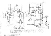
There is a design die to spectral that uses the same topology at page 211 but it doesn't explain anything.
Plus, i don't see any compensation cap on the schematic: is that possible?
I will look carefully through the book to search for a detailed implementation of the balance VAS.
In case, do you know the chapter you are referring to?
I do agree with you with the hint of starting simpler...therefore i stepped back and took all the cascoding and current gen out.
NP schematics are very nice.
The only phono stage he has it's the ONO.
It's not a low feedback design.
Stefanoo said:
NP schematics are very nice.
The only phono stage he has it's the ONO.
It's not a low feedback design.
A lot of Pearl builders will argue with this.
Stefanoo said:
I can see on this circuit that there is a split RIAA as well.
No.
Stefanoo said:
Second stage the Balance VAS stage, cascoded(bootstrapped?!..man i still don't catch the bootstrap config), no current mirror.
Anyways on the VAS stage: is the output (2SC959) a simple common emitter follower config (?!) with low output impedance, is it right?
Your analysis is not correct.
A similar circuit without cascoding
Attachments
what does TR7 on the first half of the circuit (same thing on the second half)?
It seems it bias the output emmiter follower, but it doesn't look like a current source as the current varies proportionally with the input signal.
It seems it bias the output emmiter follower, but it doesn't look like a current source as the current varies proportionally with the input signal.
analog_sa said:Not sure what the exact background is but looking at the 560k input resistor i would assume this circuit works with a step-up transformer. Never claimed it was excellent for noise or in any other respect.
The input resistor is my last concern regarding noise. The feedback resistor (470ohm), the cascode supply (not decoupled), the CCS happily multiplying the zener (not decoupled) noise and injecting current noise in the common mode, so that any mismatch in the JFETs (even 1%) will grossly impact the output, the differential stage (3dB more noise than the single ended), did I miss something?
A quick calculation shows this thing anywhere between 20 and 40 nV/rtHz noise, clearly audible hiss even in modest efficiency speakers. Then what's the point of using 2SK389? In fact, for MM or MC with stepup transformer you can do 8-10 nV/rtHz with a single 4532 opamp worth 50 cents.
This thread is symptomatic to what I call "lets throw something together, and if if it does not work, somebody is bound to come to my aid, rubbish it may be, but I have simulated it, so it should work".
I have no quarrel with people who seek advice with their concoctions, but seriously, people, have you seen those who rely entirely upon their GPS navigators, only to end up in the middle of a river. In order to make a good audio circuit, it is not enough to simulate something hacked together from several sources, and hope it will be Gods gift to the audio community. At least you got to have a basic understanding of electronics. I don`t think the author of this thread has that knowledge, and furthermore, he is not alone, diyaudio are full of people trying to freewheel upon other peoples knowledge. Simulators should be left to those who can use them.
Regards
Roar
Hi Roar,
what can I say?
I saw lots of people on the forum underestimate simulators.
Just keep in mind that these huge programs are made by great professionals and furthermore are based on precise and correct mathematical/physic models of the devices.
The result you can get can be very precise but other times the simulator can't predict the real behavior.
I strongly think that it is a good tool that doesn't work by itself.
If you say that simulators are for stupids or that have to be chucked you are saying basically that all the people who have worked for these things would better be off doing other things other than that....and i am sorry....but i DO NOT agree with you.
If you have noticed I have specified that simulator shows good behavior but real implementation wasn't which means that after have developed the circuit i tried it.
Before putting and merging and hack as you said...bloocks...i though how the circuit could work together and conceptually it worked on my mind....it's not like burst out the first couple of blocks i saw around and connect them together.......oh well!
So since conceptually worked and simulator shows correct result...plus i got people on the forum telling me that the circuit works....that's why i still keep trying!
Last but not less important...circuit are thoughts before hands tried and auditioned.
If they don't sound well....research the reason of why and change...and listen....
ahhh...and thank you for accredit me at least the basic understanding of electronics.............which means that my 32 exames for EE weren't a complete waste of time..........no pun intended 🙂
Stefanoo,
Now I see why your approach is so dourly technical.my 32 exames for EE weren't a complete waste of time
syn08 said:
The input resistor is my last concern regarding noise.
The value of the input resistor indicates there is no cartridge directly connected but rather a (1:20?) step-up. Which makes the noise performance acceptable.
analog_sa said:The value of the input resistor indicates there is no cartridge directly connected but rather a (1:20?) step-up. Which makes the noise performance acceptable.
The value of the input resistor indicates a poor design. The input stage has a LF gain of over 1800, which translates (if the RIAA is correct, I haven't checked) to a gain of 180 at 1KHz. The second stage has a minimum gain of 2.8 so the overall minimum gain is 504 (53dB). Way to much for a MC with 10:1 stepup or even for MM (and that's again on the minimum gain setting!). The headroom is also very low, given the +/- 10.5V supplies.
Using two expensive pairs of matched JFETs doesn't make any sense here.
syn08 said:
Using two expensive pairs of matched JFETs doesn't make any sense here.
I posted the circuit not as an example of a great, low noise design but rather as an example for a differential VAS as per Stefano's request. What is the point of discussing any other attributes this circuit may or may not possess? Did anyone suggest this as a great circuit to build?
- Status
- Not open for further replies.
- Home
- Amplifiers
- Solid State
- Moving Coil preamp design