paul joyce said:
Stefanoo, the bode plot tells us some useful information:
1) The compensation of C24 (or C3 in your original schematic) is VERY agressive, since the amplifier open loop resonse is rolling off below 1Hz! If you start your plot at 0.1Hz (or even lower) you should see the gain starting to flatten out.
2) The dB value of the loop gain is how much feedback you have at each frequency.
3) Where the loop gain falls to 0dB, you have -90 degrees of phase shift - so phase margin is 90 degrees. You need to try this at the other end of the RIAA gain extreme, by reducing the feedback resistors to 1/100th of their current values.
The dc voltage across R4 is fixed by dc feedback for a given output voltage. Changing R4 will force an imbalance in current in the differential pair, but using this to tweak offset is crude.
Better to put a pot in between the input pair source connections with the wiper to the current source. This allows the input offset voltage to be directly controlled, and the resistance will also reduce DC drift, and reduce the Gm and improve the linearity of the input stage. Self shows this in his book, although he is using bipolars.
R56 should be bypassed so that the output gates see the same impedance at high frequencies, as this resistor is only there for DC bias.
Adding a resistor to ground at Q6 collector will allow you to define the open loop voltage gain. Currently, this impedance is only defined by the transistors themselves. If you connected a resistor from Q6 collector to J1B gate via cap, you could then have an internal feedback loop to define the open loop gain.
You can also add a resistor in series with Q3 source to reduce the Gm of the VAS, which will also reduce the DC drift.
Doug Self's technique of meausuring the voltage across the diff pair inputs can be done (in a closed loop, this is the error voltage, so dividing the output voltage by this gives you the open loop gain. It's a very tiny voltage though, so would have to be amplified. Example - if your open loop gain is 100dB, an output voltage of 10V would mean this differential voltage is only 0.1mV!
the signal at R4 is the amplified error signal, so it's a little easier to see.
Doug Self's idea of loading differential pair output with a current mirror allows you to obtain the full gain of the diff pair (i.e Gm x R4 instead of Gm/2 x R4). Personally, I like a Differential VAS as it is more linear than the single ended version, and in your case has less DC drift.
Hi Paul,
sorry for the delay.
I didn't leave the project i was just trying to run the circuit with a balance VAS stage since you gave the hint that a balance VAS would help DC and it's more linear.
So i first tried to simulate.
When i got it working on PSpice i tried to build it.
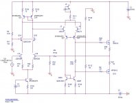
I have attached the schematic.
I can't understand why the generator current made with the Jfet doesn't properly operate without R111....anyways.....
this circuit doesn't work in practice and i don't understand why!
Can you give me some hint? is there any gross mistake i don't see?
I would be very excited to try this one out.....ggrrrr!!!
I haven't purposly placed any compansation capacitor since my first goal was to run the balance VAS topology and then find the appropriate compensation cap's value.
Any suggestion is welcome...
thank you for your attention.
Attachments
In ARTA you can use a mic compensation file to "fool" the system with a RIAA-mic file. It is on ARTA's web site. I think you can do the same in SpectraPLUS.
Sigurd
Sigurd
Stefanoo said:
As soon as the soundcard will get here I will try them both.
The RIAA generator is a very nice tool.
Just wondering:
Is it possible with SpectraPlus to do a post analyze of the frequency response and build a RIAA math function and plot the error?
Hi,
i prefer not to use opamp.
The phono will be a discrete design.
Still, i can't understand where the design fails....i mean...it simulates just fine but it doesn't work in practice...
i prefer not to use opamp.
The phono will be a discrete design.
Still, i can't understand where the design fails....i mean...it simulates just fine but it doesn't work in practice...
Stefanoo said:Hi,
i prefer not to use opamp.
The phono will be a discrete design.
Still, i can't understand where the design fails....i mean...it simulates just fine but it doesn't work in practice...
You need to put forward the completed design for us to have a look at. Your previous cct diagram shows voltage sources which need extra components.
the voltage reference (the V4 1.6V) is simply made by a diode led with a 8k current limiting resistor to ground.
What have you done so far ?
Have you been around the cct with a multimeter checking voltages ?
Have you got a scope to check voltages ?
Have you been around the cct with a multimeter checking voltages ?
Have you got a scope to check voltages ?
emmm... of course i have got a scope 🙂 i am not using it now since it's 1.10AM and i am typing on the bed🙂 buuut i will again tomorrow. 🙂
Stefanoo said:emmm... of course i have got a scope 🙂 i am not using it now since it's 1.10AM and i am typing on the bed🙂 buuut i will again tomorrow. 🙂
OK let me know how you get on.....
Sigurd Ruschkow said:In ARTA you can use a mic compensation file to "fool" the system with a RIAA-mic file. It is on ARTA's web site. I think you can do the same in SpectraPLUS.
Sigurd
Sigurd,
just last thought before going to bed....
looking through SpectraPlus and the manual, i have seen that under the menu Optio-scaling, there is the option Microphone compensation which allows you to compensate for any curve you want.
Apparently there is a procedure for compensating the response curve of your soundcard.
I am wondering if it would be possible to make it flat on the entire band (up to 90KHz.
Since i saw the response for the Emu track and looks handsome within 20-20KHz and before and after that falls off...with this compensation it might be possible to compensate for that normal cutoff freq...i think....mmmm....interesting!
I don't know if you have ever use this feature or nor...but i think it might be worth exploring it.
alright...time to hit the bed 🙂
Stefano,Stefanoo said:
Hi Paul,
sorry for the delay.
I didn't leave the project i was just trying to run the circuit with a balance VAS stage since you gave the hint that a balance VAS would help DC and it's more linear.
So i first tried to simulate.
When i got it working on PSpice i tried to build it.
I have attached the schematic.
I can't understand why the generator current made with the Jfet doesn't properly operate without R111....anyways.....
this circuit doesn't work in practice and i don't understand why!
Can you give me some hint? is there any gross mistake i don't see?
I would be very excited to try this one out.....ggrrrr!!!
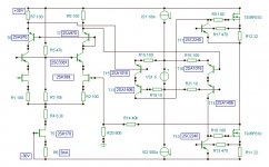
the current mirror on the input diff pair is only used for a single ended output. Since your are following the first differential pair with a second pair, you only need resistive loads on the first stage. R103 and R104 need to be much larger to generate enough bias for the next stage - probably in the 2k range.
Next I think J2 will not provide a well defined current. Simply by tying the gate to the source the device current will be Idss, which from the device spec can be anything from 2.6 to 20mA! Move the resistor R111 between the source and gate connections, and adjust its value for the current you want - maybe try this on its own first.
Hi Paul,
I did what you suggested but the circuit still seems to not properly work.
I just don't get it right yet.
In fact, it works at low voltages after proper adjustmets of the output stage's bias...but it's strange.
I will keep on working on it.
If anybody wants to follow this circuit and decides to try building it and suggestes some updates...it would be great!
Stefanoo said:Hi Paul,
I did what you suggested but the circuit still seems to not properly work.
I just don't get it right yet.
In fact, it works at low voltages after proper adjustmets of the output stage's bias...but it's strange.
I will keep on working on it.
If anybody wants to follow this circuit and decides to try building it and suggestes some updates...it would be great!
Stefano,
Do you have any feedback compensation anywhere- there was no caps in the schematic. Since this is now differential, you could put a cap between Q1 collectors, as a starting point. A circuit that has feedback instability can do some strange things!
Hi lumba,
sorry, did you simulate and/or built the circuit you attached?
Also, it seems to me that complexity has increased from the circuit I have posted.
I have tried to simulate it but i couldn't get it working.
sorry, did you simulate and/or built the circuit you attached?
Also, it seems to me that complexity has increased from the circuit I have posted.
I have tried to simulate it but i couldn't get it working.
paul joyce said:
Stefano,
Do you have any feedback compensation anywhere- there was no caps in the schematic. Since this is now differential, you could put a cap between Q1 collectors, as a starting point. A circuit that has feedback instability can do some strange things!
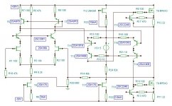
I have tried to build it without any cascoding and without active load at the front end.
The strange thing is that if i modify the bias at the output devices throug the resistor on the second differential....the output increased or decreases...and at a certain point it shuts down if the input voltage increases or i have strange behaviours.....
i have tried to put some caps along but couldn't get it working...i don't know....
if you have a chance and you would like too...or anybody here...would like to...could build the circuit with me and kinda of working it around together...that would be awesome...
Stefanoo said:
I have tried to build it without any cascoding and without active load at the front end.
The strange thing is that if i modify the bias at the output devices throug the resistor on the second differential....the output increased or decreases...and at a certain point it shuts down if the input voltage increases or i have strange behaviours.....
i have tried to put some caps along but couldn't get it working...i don't know....
if you have a chance and you would like too...or anybody here...would like to...could build the circuit with me and kinda of working it around together...that would be awesome...
Stefano, I do not have all these parts to build the circuit. There is nothing special about this circuit - it has been around for >30 years. One other issue is Q26 and Q27 bases are biased with a negative voltage. This needs to be a positive bias >+20V.
paul joyce said:
Stefano, I do not have all these parts to build the circuit. There is nothing special about this circuit - it has been around for >30 years. One other issue is Q26 and Q27 bases are biased with a negative voltage. This needs to be a positive bias >+20V.
Hi paul,
i mean...the circuit can also be built with simple and general purpose NPN/PNP device as evaluation...but don't worry...
Actually I have never seen this exact circuit around and if you did and you wis, pleae please point it out as there might be suggestions on how to run it 🙂 .
The principle of the circuit is nothing new, of course and i don't even know if it will sound nice or not.
Anyways...bout the Q26/27 i know...it is a mistake on the schematic.
I will up-to-date it and post it again once i have tweked and properly run.
When you meant to say that the circuit is nothing special, you meant to say that there are better topologies that can be used? if so, would you like to give any suggestion?
Hope you will have a good day.
Best.
any advice is of course very welcome.
Lumba Ogir said:Stefanoo,
it`s just drawn hurriedly and erroneously, I apologize, can be simplified at the expense of linearity.
Hi Lumba,
don't worry the schematic is drawn really clear.
I still don't understand a couple of things...as for example why you choose a not symmetric output stage and the way you bias the output stage.
The new schematic you have attached is identical to the previous one except you have drawn the little CCS instead of leaving the symbols...so i guess it still doesn't work.
If you haven't simulated it yet, you can try yourself in case i made some mistakes on simulating it.
Thank you for your schematic anyways.
- Status
- Not open for further replies.
- Home
- Amplifiers
- Solid State
- Moving Coil preamp design