Back on track to madness 
I know now why the madness did not work.
The basic susy circuit works like always only one pair of the transistors carries its half wave of the signal.
For classA all transistors have to carry the signal all the time.
So I will change the basic circuit and add my madness, there are different ways that need to be explored.
Huh?
You lost me on that last one, Bernhard.
In SUSY, each half(?) tries to carry *exactly* the same signal, just out of phase so that when they meet at the load, they match perfectly and add. Differences create a differental - and thus are eliminated by the X feedback.
(My simple understanding..)
Still can be class A, AB, B or whatever. Probably could be D too now that I think about it. Now that would be different.
Huhhh...
Misunderstanding, I meant between up and down, not left and right.
If you just look on one side, there is the idle current through both transistors.
If a positive or negative halfwave comes, the current rises in one transistor.
But it doesn't fall in the other one.
So always only one transistor is busy, however you increase the idle current, it doesn't matter.
At least thats my understanding from watching the sim.
By connecting the Op-output to the transistors (instead of the Op-rails), one current will rise and the other one will fall at the same time.
If the idle current remains very small, the amp will be clipping soon even on small signals.
What I like to do, is to have the low idle current at small signals and increase it proportional to the signal level to high idle current at large signals.
And I could need some help 🙄
You all know, I have very little knowledge of amp building... 🙄
Maybe this is what I was looking for in my early madness circuits:
Idle current per output Fet is 200mA, which means, normally when the output current exceeds 200mA, the circuit goes to classB, because two fets run out of current.
Now when you look at output Fet N1, you see that the gate voltage goes higher if the op amps draw current.
On the positive halfwave one op amp draws current and on the negative the other one.
Normally if the output of op amp X1 goes negative, Fet N1 will not conduct current anymore because its gate voltage will go negative too.
But because op amp X2 draws current, Fet P1 conducts more current and the negative output voltage of op amp X1 can not pull down the gate of the output Fet N1.
It is hard for me to explain, I hope you all understand... 🙄
Now is this what I liked, ClassA with dynamic idle current = Class dynamic A ?
Or is it pure nonsense ?
Or just some ClassAB which could be achieved with a more simple circuit ?
It is not the final circuit, the X-connections are still missing, rails for the op amps are much too high...
Also the gate voltage of Fet N1 goes up even more when the output of opamp X1 goes positive, so Fet N1 conducts even more current.
I think this is not necessary, so half of the connections to the op amp supplys can be left out.
Bernhard said:
Or is it pure nonsense ?
Yes... It has a sense.
Pass's Aleph current source provides a dynamic Q-point, for example.
Yes... I want to see your good sounding amp of simple circuit and high power. 🙂
JH
JH & Netlist,
🙁 I found a problem 🙁
It applies to all circuits.
Example:
In my high power circuit the idle is 210mA.
But the current in the upper two 0.22 ohm resistors goes down to 60mA when the sine is negative.
In the lower two resistors the current goes only to 210mA when the sine is positive. How it should be.
I did not check the real circuit yet, the problem is in the sim.
Also the rail currents of the LM are not equal.
I would be interested what you see on the scope or in the sim.
Ok, the circuits develop
Where are You all ? Its getting real interesting
- Now the two-transistor gain stages need only one transistor.
- One circuit is normal classA push-pull and can be biased with fixed high idle current and lots of heat
or
with small basic current that can/must be increased with output power.
- The other circuit is also classA push-pull biased 300mA per Fet and automatically prevents the Fets from running out of current.
New schematics soon
Hey, I have learned so much since this thread has started and its getting faster and faster 😀
Hi Bernhard
Just to clear things up for my simple mind, I some questions.
From reading your posts, I gather that you are trying to modulate the Bias if the output trannies so they stay in class A all the time, yet use as low a current as possible. This sounds like a fine idea, and I ssume you are using another amp like stage to increase the bias on the outputs as the current demands get higher. Is this the case?
Surely, unless you have a very fast amp to increase the bias, it will always be lagging behind the input, and lagging after, (probably not so much of a problem as this only wastes energy through heat). Would this increase distortion on transients? Could you increase the bias above the base level so much that the hysteresis of the circuit is not affected?
This sounds like a fascinating circuit, but I am afraid my technical knowledge is a little lacking to assist much- I can only point out obvious stuff, so if you already thought of this I apologise😉
Hi pinkmouse,
yes, i was thinking about timing problem too.
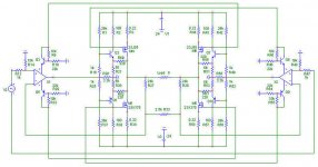
Look at the circuit:
The bias modulation goes straight from the op amp rails to the output Fets
The signal has to pass another transistor stage, so who is first, the bias modulation or the signal ?
I guess the problem is not worse than that of feedback.
Still I am not shure if this all makes sense...
First new circuit comes in about one hour 🙂
yes, i was thinking about timing problem too.
Look at the circuit:
The bias modulation goes straight from the op amp rails to the output Fets
The signal has to pass another transistor stage, so who is first, the bias modulation or the signal ?
I guess the problem is not worse than that of feedback.
Still I am not shure if this all makes sense...
First new circuit comes in about one hour 🙂
Ok, I think I'm getting my head around this...🙂
Ignoring the RH side for the moment, Q1 and Q3 provide the bias to IC1 to force that into class A, Q5/Q8, and Q6/Q7 are a voltage amp stage, and P1 and N2 provide the variable bias to N1 and P2 the outputs.
Correct so far?
Ignoring the RH side for the moment, Q1 and Q3 provide the bias to IC1 to force that into class A, Q5/Q8, and Q6/Q7 are a voltage amp stage, and P1 and N2 provide the variable bias to N1 and P2 the outputs.
Correct so far?
pinkmouse said:Ok, I think I'm getting my head around this...🙂
Ignoring the RH side for the moment, Q1 and Q3 provide the bias to IC1 to force that into class A, Q5/Q8, and Q6/Q7 are a voltage amp stage, and P1 and N2 provide the variable bias to N1 and P2 the outputs.
Correct so far?
Old schematic post 725:
Q1 and Q3 are voltage regulators that reduce the 24V rails to 15V for the op amps.
Q5/Q8, and Q6/Q7 are a voltage amp stage, right, because the 15V opamps can not drive the 24V output stages directly.
Yes, P1 and N2 provide the variable bias to N1 and P2 the outputs.
(One question is: Do the op amps work in classA ???)
When there is a positive halfwave, the the current of the +rail of op amp X1 increases, so the current through R2 increases and the voltage at the gate of P1 gets lower, so P1 conducts more and the bias of N1 gets higher.
This is nonsense, but also if the other side (right) draws more current, the bias of N1 gets higher. And this is the case when there is a negative halfwave on the left side, so...
Ok, lets look at the new better circuit post 732:
Current through M4 gets higher on positive halfwaves and lower on negative halfwaves.
Positive is no problem, the current can go as high as it wishes.
But negative is a problem, the current can not become negative, so if the bias is not high enough, the current will go to zero.
Imagine there would be only 300mA and a negative halfwave big enough that M4 would not conduct any current no more.
Now the current flows through M1 and M6. M4 and M5 do not conduct anymore.
The gate current for M6 is provided by the positive rail of X2.
More current through R2 and M4 conducts current again.
Same for M5.
Here we go.
The currents through the Fets can not go below idle if the circuit is adjusted right.
It can be adjusted also that the current even goes up at negative, but this again is nonsense.
Hmmm, the original circuit does the same ????
When leaving out the connections to the op rails, the circuit can be normal biased in classA, or coupled to a relais pot to adjust the bias to the output power automatically and save heat
Bernhard said:
Where are You... ?
I'm staying in Shanghai, leaving all hobby tools at home. 🙁
I read your posts with great intersts. 🙂
JH
Bernhard
Thanks for the explanation, I think I understand a little better now!🙂
Two things come to mind, again I apologise if they are stupid, and they are meant to be constructive!🙂
Are you over complicating things by crossing over the variable bias to the opposite side? Surely you gain nothing by this, as the error correction using the X from the opamp is going to be insignificant in relation to the main signal?
Would there be a better place to take the variable bias control signal from, as I am not familiar with the innards of op amps, but I can't believe that the current drain on the input is both as fast and in proportion to the output as you think, because of all the extra circuitry within the amp?
Bernhard said:pinkmouse,
I don't know 😕
Bernhard, if I knew, I would answer. I'm stunned by the amount of generated creativity, but only have enough skills to give you inaccurate replies.
/Hugo 😉
Netlist,
it seems only Nelson knows the answers.
But, do you see the same effect like me,
that in the upper 0.XX ohm resistors, the current goes below idle @ negative halfwaves, but not in the lower ones @ positive.
Also the LM rails + and - do not draw the same idle current.
I got many new ideas
it seems only Nelson knows the answers.
But, do you see the same effect like me,
that in the upper 0.XX ohm resistors, the current goes below idle @ negative halfwaves, but not in the lower ones @ positive.
Also the LM rails + and - do not draw the same idle current.
I got many new ideas
Bernhard said:
But, do you see the same effect like me,
that in the upper 0.XX ohm resistors, the current goes below idle @ negative halfwaves, but not in the lower ones @ positive.
Also the LM rails + and - do not draw the same idle current.
I remember having that problem in reality, not with the sim.
It is mentioned somewhere in this thread. I'll try to remember what was the cause of it. But this was another, less complicated circuit.
Mail me the model.
/Hugo 🙂
- Status
- Not open for further replies.
- Home
- Amplifiers
- Pass Labs
- Monolithic SuperSymmetry with Current Feedback