Hi All,
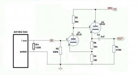
I have a 6DJ8 tube preamplifier kit that I would like to modify to perform as a tube output stage for a AD1862 DAC chip using a passive ressistor for the I/U conversion.
the AD1862 output is 1ma (+/-).
I'll appreciate your suggstions for optimizing the following schematics.
Cheers
I have a 6DJ8 tube preamplifier kit that I would like to modify to perform as a tube output stage for a AD1862 DAC chip using a passive ressistor for the I/U conversion.
the AD1862 output is 1ma (+/-).
I'll appreciate your suggstions for optimizing the following schematics.
Cheers
Attachments
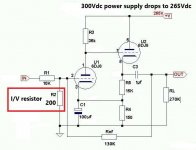
What is R1? Current output DACs have very little voltage compliance (typically +/-0.5V), R1 is certainly a mistake in this context.
The datasheet for the AD1862 explicitly states the output should be to a summing junction at virtual ground - i.e. its explicitly designed for an opamp topology, not a passive resistance. From the datasheet:
All current output DACs perform most linearly in this mode (summing to virtual ground) anyway.
The datasheet for the AD1862 explicitly states the output should be to a summing junction at virtual ground - i.e. its explicitly designed for an opamp topology, not a passive resistance. From the datasheet:
Alas the meaning of "approximately" isn't given, nor is the voltage compliance spec.The output of the AD1862 is intended to drive the summing junction of an external current-to-voltage conversion op amp. Therefore, the voltage on the output current pin of the AD1862 should be approximately the same as that on the AGND pin of the device.
All current output DACs perform most linearly in this mode (summing to virtual ground) anyway.
Ad 1862 works very well into passive I/v and a valve output stage. I used 330r with mine. The issue here is you've got a stage with a lot of gain and you've got your load resistor in the wrong place
Juancho I’m considering lowering the I/U resistor value even more so there there is a need for the extra gain to get close to 2V output, kindly correct me if I’m wrong.
Where the load resistor should be placed?
Mark what is your suggestion?
Thanks
Where the load resistor should be placed?
Mark what is your suggestion?
Thanks
What is R1? Current output DACs have very little voltage compliance (typically +/-0.5V), R1 is certainly a mistake in this context.
You are right, I forgot to remove it from the drawing.
Attachments
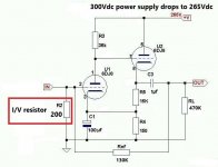
BTW What is the purpose of the resistor marked Rnf (130k)?
I assume it is left over from when this was a Voltage-to-Voltage amplifier. 130K against the 10K input resistor implies a gain of 13V/V. Since tube gain is not a lot more, maybe really a gain of 10 or 7 V/V. A reasonable line-amp.
> optimizing the following schematics.
An I/V amp is really a different thing than a V/V amp.
But I guess you HAVE a circuit board and parts in hand. And you may not want to tear them up and do it another way. And yes, passive resistor for the I/U conversion can work fine. Do this:
Attachments
Thank you.
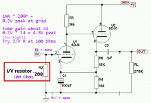
I've tried 100R resistor but when I compare (by ear) it's sound output level to another DAC that I have it sounds lower in volume.
What is the "other way" that you have in mind?
I've tried 100R resistor but when I compare (by ear) it's sound output level to another DAC that I have it sounds lower in volume.
What is the "other way" that you have in mind?
RNF is the resistor for negative feedback. It also lowers the input impedance by forming a summing junction.
Should I leave it or remove it?what is the advantage/disadvantage of using it for my purpose?
Thanks
Thanks
I removed the 100uf capacitor (as I understand it's a bypass capacitor) , as far as I know a bypass capacitor should change the gain and output impedance, is it a bypass capacitor?
I'm asking because I couldn't hear any difference and there is no change in the gain.
I'm asking because I couldn't hear any difference and there is no change in the gain.
RNF is the resistor for negative feedback. It also lowers the input impedance by forming a summing junction.
True in theory, but with 200 ohm (or 100 ohm) across the input, there is so little loop gain that it hardly does anything. Hence the recommendation to remove it.
Should I leave it or remove it?what is the advantage/disadvantage of using it for my purpose?
Thanks
As the feedback loop has practically no loop gain, you probably won't notice any difference.
If I understand correctly the drawing is basically a common cathode circuit connected to a cathode follower, if it is correct then shouldn't R4 and R5 be connected the otherway around so R4 will be connected to the cathode as a bias resistor (Rb) and R5 connected to the R4 junction and ground to act as Rk resistor?
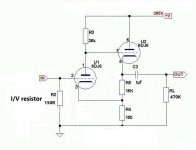
R4 is the cathode/bias resistor in that version, and it also is part of a compound circuit so is shared with the other triode.
Thanks.
I soldered the I/U resistor (SMD resistor) directly on the AD1862 I out and AGND legs and added a Rg 300K ressistor between the input and GND and changed the output capacitor to 3uF.
How do you think I can optimize this circuit further?
I noticed that in quiet tracks or when there is silence between tracks I can hear background noise, what can be the reason for that noise?
Attachments

Last edited:
Question:
Why do you have positive feedback introduced from the cathode follower to the cathode of the first stage ECC88 (pin 3)?
It seems to me the problem here is an excess of gain.
Why not connect R5 from U2 pin 8 straight to ground, and connect R4 straight from U1 pin 3 to ground? That way you get a little cathode degeneration into U1, reducing the gain a bit, and lowering THD a bit.
U1 is driving the grid of the cathode follower U2, which has a very high input impedance. Therefore, the increase in rp of U1 from cathode degeneration is a non-issue.
Or maybe I'm completely off base here. Just curious...
--
- Home
- Amplifiers
- Tubes / Valves
- modifing 6DJ8 kit for DAC output stage