Quoting Mark Johnson in his post on his Quasimodo snubber test jig, https://www.diyaudio.com/community/...rmer-snubber-using-quasimodo-test-jig.243100/, "A power transformer snubber is a wonderful thing for reducing or eliminating RFI from rectifier-induced LCR ringing."
Edit: Just a note. I don't have snubbers installed in my test power supply. Snubbers will not solve 120 Hz noise problems. Look for grounding issues, current loop areas, and component layout.
Edit: Just a note. I don't have snubbers installed in my test power supply. Snubbers will not solve 120 Hz noise problems. Look for grounding issues, current loop areas, and component layout.
Last edited:
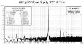
I adjusted the cascode voltages in the voltage amplifier, lowering the SiC JFET Vds to 17.1V. Previously, it was at 19.5V. This didn't change the distortion of the lower voltage outputs, but at 84Vpp out, the 1 kHz THD dropped to 0.0037% from 0.0051%.
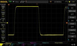
I also checked on the oscilloscope the output of a 19.5 kHz square wave. I have a 15p capacitor across the feedback resistor. The leading edge of the square wave is a bit rounded.
I also checked on the oscilloscope the output of a 19.5 kHz square wave. I have a 15p capacitor across the feedback resistor. The leading edge of the square wave is a bit rounded.
Attachments

would you please share the Gerber file of the preamp?I've got the PCB design for the United SiC power JFET voltage amplifier (preamp) pretty well finished. I can probably leave it as is, but since JLCPCB is still on holidays until the weekend, I may still tinker with the layout a bit.
The PCB will be 114 mm x 60 mm, so it shouldn't be very expensive to produce. There are provisions for heatsinking the JFET and MOSFET which is a good idea since they each dissipate several watts. The footprint for the coupling capacitors is 32mm x 17mm, so some decent film capacitors can be used.
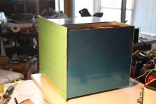
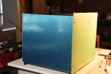
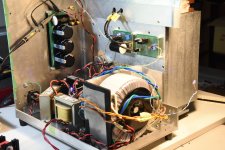
I've been slowly working on this amp over the last little while, and today, I reached a milestone of sorts. The case for the right channel monoblock is substantially complete. I ordered the cut-to-size aluminum plates for the front, back, sides, and top from Metal Supermarkets and bolted it all together with aluminum angles and bar. Lots of drilling and tapping. Also, drilled and tapped the bottom plate and heatsink for mounting PCBs and other components. I still need to drill the back panel for the usual things plus a PCB for the output capacitors, and few a holes here and there, but that's easy stuff.
After thinking a lot on how to lower my power supply voltage from around 120V to 90V, I decided that the easiest way was to get new power transformers. So, that's what I did. While I was doing that, I also decided to save my 22 mfd 80V capacitors for another build (kind of wasted connected in series) and bought a bunch of 3.3 mfd 160V capacitors. In quantities of more than 10, the price was not too bad. In the end, the CLCLC filtration is basically the same but I saved a bit of space and have most of the 60V power supply for another build. Those parts will come in handy for my United SiC power JFET power amp.
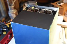
The aluminum case looks quite plain and simple now, but my plan is to add a thicker and wider wood panel to the front and paint the side panels black (or maybe use stick-on black vinyl). A piece of black painted plastic grating over the fan opening is also in the plans. This case is quite large so hopefully these cosmetic additions will improve the big metal box look.
After thinking a lot on how to lower my power supply voltage from around 120V to 90V, I decided that the easiest way was to get new power transformers. So, that's what I did. While I was doing that, I also decided to save my 22 mfd 80V capacitors for another build (kind of wasted connected in series) and bought a bunch of 3.3 mfd 160V capacitors. In quantities of more than 10, the price was not too bad. In the end, the CLCLC filtration is basically the same but I saved a bit of space and have most of the 60V power supply for another build. Those parts will come in handy for my United SiC power JFET power amp.
The aluminum case looks quite plain and simple now, but my plan is to add a thicker and wider wood panel to the front and paint the side panels black (or maybe use stick-on black vinyl). A piece of black painted plastic grating over the fan opening is also in the plans. This case is quite large so hopefully these cosmetic additions will improve the big metal box look.
Attachments


Nice work so far.
I've been considering building class a monoblocks in such a manor with the heatsinks internal like that.
Very inspirational, I look forward to seeing how it turns out
I've been considering building class a monoblocks in such a manor with the heatsinks internal like that.
Very inspirational, I look forward to seeing how it turns out
Yes. Still planning on it. I'm aiming to just hit the 100 watt mark. Achieving the 100 watts is not a problem. The issue is how hot is the SIT getting. I think I've got enough cooling now that it will work. Maybe, I'll dial it back to 95 or 90 watts after the thrill of 100 watts fades.
I finished assembling my power supply. It's been tested with a 40 ohm resistor load and the output settles in at 103V. This works out to just under 2.6 amps which is pretty well what my target is.
I bought new AN-6440 power transformers from AnTek. These are rated at 600VA with 2 x 40VAC, 18VAC, and 12VAC secondaries. The original 2 x 50VAC AnTek transformers would have required extra costs and work to drop 20VDC from the power supply output. In the long run, proper sized transformers were easier to work with and I can reuse the transformers for a future build.
That was also the reason I saved the 22mF 80V filter capacitors and bought new 3.3mF 160V capacitors. Using two 80V caps in series to get the voltage requirements sacrificed a lot of capacitance. Of course, if I wasn't planning on build another amp with a 60V power supply, it would be different story.
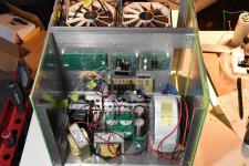
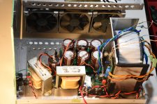
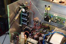
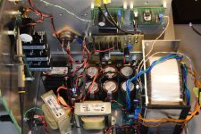
The main power supply is CLCLC. This consists of: 9.9mF - 10mH - 9.9mF - 28mH - 3.3mF. PSUDII simulations predicted 100VDC with 0.48mVpp of ripple. This works out to less than 0.2mVrms. I have found that PSUDII ripple predictions have correlated well with actual finished amplifier noise performance, so I'm confident that this will work out. The capacitance in the filters is lower than what I normally use, but the extra inductor makes up for that. I was lucky to get the 28mH inductors at a very good price.
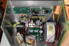
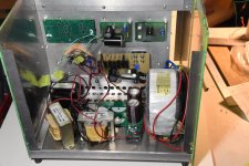
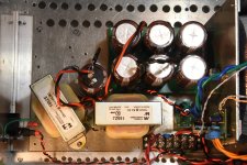
I made PCBs for transformer snubber components and for the CLC filter section and that cleaned up the chassis layout a lot. There is still the voltage amplifier load inductor to add to the bottom plate and that will take up the remaining space.
I weighed the the two main parts of the amp under construction to get an idea of its final weight. The case part with the power supply weighs in at about 26 lbs and the heatsink assembly is about 20 lbs. It looks like the finished weight of a monoblock will be close to 50 lbs (23 kg). It's a good thing that I didn't purchase 3/8 inch aluminum plate for the case face plate.
I bought new AN-6440 power transformers from AnTek. These are rated at 600VA with 2 x 40VAC, 18VAC, and 12VAC secondaries. The original 2 x 50VAC AnTek transformers would have required extra costs and work to drop 20VDC from the power supply output. In the long run, proper sized transformers were easier to work with and I can reuse the transformers for a future build.
That was also the reason I saved the 22mF 80V filter capacitors and bought new 3.3mF 160V capacitors. Using two 80V caps in series to get the voltage requirements sacrificed a lot of capacitance. Of course, if I wasn't planning on build another amp with a 60V power supply, it would be different story.
The main power supply is CLCLC. This consists of: 9.9mF - 10mH - 9.9mF - 28mH - 3.3mF. PSUDII simulations predicted 100VDC with 0.48mVpp of ripple. This works out to less than 0.2mVrms. I have found that PSUDII ripple predictions have correlated well with actual finished amplifier noise performance, so I'm confident that this will work out. The capacitance in the filters is lower than what I normally use, but the extra inductor makes up for that. I was lucky to get the 28mH inductors at a very good price.
I made PCBs for transformer snubber components and for the CLC filter section and that cleaned up the chassis layout a lot. There is still the voltage amplifier load inductor to add to the bottom plate and that will take up the remaining space.
I weighed the the two main parts of the amp under construction to get an idea of its final weight. The case part with the power supply weighs in at about 26 lbs and the heatsink assembly is about 20 lbs. It looks like the finished weight of a monoblock will be close to 50 lbs (23 kg). It's a good thing that I didn't purchase 3/8 inch aluminum plate for the case face plate.
Attachments
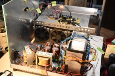
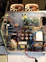
Over the last week, I installed the complete output stage into the case. After much checking of the wiring, I hooked the amp to a dummy load, signal generator, oscilloscope, and slowly brought it to life with a Variac. At about 12VDC at the power supply output, the oscilloscope showed a nice sine wave. As I increased the power supply voltage to full output, no unpleasant events took place.
A few quick measurements of the SIT revealed Vds = 52V and Iq = 2.3A. The works out to 120 watts dissipation.
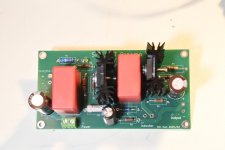
I also finished a final version of the SiC voltage amp. I just need to test it and install it in the amp. There's just enough room at the top left of the heatsink for it.
A few quick measurements of the SIT revealed Vds = 52V and Iq = 2.3A. The works out to 120 watts dissipation.
I also finished a final version of the SiC voltage amp. I just need to test it and install it in the amp. There's just enough room at the top left of the heatsink for it.
Attachments
I would be worried about the safe operating area of the IXYS PFET rather than the 2SK82ES. The Token SIT hard to kill, but I have destroyed many IXYS PFETs.
The mu follower can be modified for parallel multiple FETs to distribute the power dissipation.
The mu follower can be modified for parallel multiple FETs to distribute the power dissipation.
That's good to know about the toughness of the SIT.
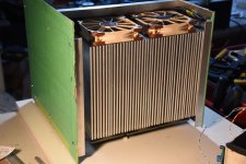
I have good airflow through the heatsink and the temperatures seem to be under control. The Noctua fans operate at full voltage in push-pull configuration and they move a lot of air.
The MOSFET is working at Vgs of 50V and 2.3A. The DC Safe Operating Area for the device shows the limit for 50V is about 15A at 25C case temperature. I think the actual case temperature is about 45C, so there would be a derating factor.
I will take some measurements to get a more accurate temperature. I just remember that it was cooler than the SIT. Of course, the MOSFET doesn't need an insulating pad so the heat flow to the heatsink encounters less resistance.
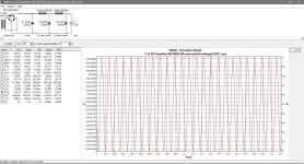
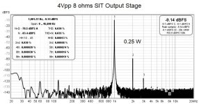
I wanted to measure the power supply noise to establish a baseline before adding the voltage amplifier to the mix. I fired up REW and fed the amp a 1 kHz sine wave and set the output to 4Vpp (0.25W / 8 ohms). The 60 Hz noise and its accompanying harmonics were evident although of low level.
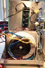
So, I starting rotating the toroid power transformer and managed to eliminate the measurable 60 Hz harmonics above 180 Hz. As well, the lower frequency harmonics dropped about 10 dB in amplitude. The attached image shows the transformer in its final orientation and the REW FFT is also attached.
I took some temperature measurements while I was in test mode. I used a thermocouple probe in direct contact with the metal surfaces and got these readings:
MOSFET flange at heatsink: 39 deg C
SIT flange at heatsink: 57 deg C
Top of heatsink: 31 deg C
It's interesting that although the MOSFET and SIT are both dissipating about 117 watts, there is a significant temperature difference. Of course, the MOSFET does not have an insulating pad between it and the heatsink.
The ambient room temperature was about 22 deg C, so the heatsink cooling is working well.
Attachments
I installed the SiC voltage amp board into the amp a few days ago and did some quick testing. The DC voltages checked out correctly, but when I added a 1 kHz signal to the input, I saw that the 4Vpp output sine wave seen on my oscilloscope was bouncing up and down at a low frequency (< 20 Hz). The amplitude of the bounce was less than 200 mV, although there were occasional larger swings.
I checked for high frequency oscillations and found nothing in the circuit beyond the environmental background levels. I thought about inadequate decoupling between stages. Nothing I tried made much difference.
One thing that I did verify though, the output stage by itself was stable. The problem was in the SiC voltage amp. I looked all the voltages in the SiC amp and found that the voltage at the drain of the common base MOSFET of the cascode was showing small voltage variations over time which would explain the symptoms.
As I was unable to solve this problem on the test bench, I fired up LTspice on my computer to see if circuit simulations would reveal anything, I found that if I zoomed in to the output signal to the millivolt level, low frequency, low amplitude oscillating behavior was evident. This millivolt level amplitude was hidden in the big picture of the several volt level of the output signal.
I looked further and found similar oscillation behavior at the input node of the amp where the input signal combined with the negative feedback loop. It appeared that there was some phase problem between the input and feedback signals.
There are three capacitors in the circuit and two are for DC voltage isolation. The third bypassed the source resistor on the SiC transistor. Looking at it now, I don't know why I added it. I didn't need more gain and the local feedback was not an issue.
So, I removed the bypass capacitor and LTspice confirmed that it was the cause. Applying this change in real life proved LTspice to be correct.
I spent several days chasing this problem, so I'm happy that it's fixed.
Attachments

- Home
- Amplifiers
- Pass Labs
- Mo' Power - 100W / 8 ohms From Tokin 2SK182ES SIT? Can't Resist the Siren's Song