That's unacceptably bad. Definitely time to move to LTSpice.
As if the ability to share your work wasn't already sufficient.😉
Best wishes
David.
Thanks David. I will attempt to make the transition as soon as possible.
Best wishes,
Ian
Hi everyone,
thank you very much for your help Dave Zan and ihan,
I've discovered that using the MJE340/MJE350 pair it's possible to plot correctly the frequency response of the VAS using dominant pole compensation.
Why that happens?
😕
That's because I've seen Michael Kiwanuka doing a similar procedure on post 63 of "TMC vs TPC vs Pure Cherry" thread.
😀
I know that in real life the amplifier should always have the feedback loop closed.
PS: I don't intend to use the MJE pair. The 2SC3503/2SA1381 could be an unstable VAS pair?
🙁
Best regards,
Daniel
thank you very much for your help Dave Zan and ihan,
I've discovered that using the MJE340/MJE350 pair it's possible to plot correctly the frequency response of the VAS using dominant pole compensation.
Why that happens?
😕
Unless you plan to add a 1GF capacitor to your actual amplifier then I don't think this is useful.
Why do you persist with this?
That's because I've seen Michael Kiwanuka doing a similar procedure on post 63 of "TMC vs TPC vs Pure Cherry" thread.
😀
I know that in real life the amplifier should always have the feedback loop closed.
PS: I don't intend to use the MJE pair. The 2SC3503/2SA1381 could be an unstable VAS pair?
🙁
Best regards,
Daniel
Attachments
I've discovered that using the MJE340/MJE350 pair it's possible to plot correctly the frequency response of the VAS using dominant pole compensation.
Why that happens?
It seems to be some problem in LTSpice rather than the specific transistor.
Sometimes I make some minor alteration and the phase reversal appears or disappears.
That's because I've seen Michael Kiwanuka doing a similar procedure on post 63 of "TMC vs TPC vs Pure Cherry" thread.
Perhaps Mike's way is better if you have to explain it to Mike.
I can help you better if you do it the way I have tested.
...I don't intend to use the MJE pair. The 2SC3503/2SA1381 could be an unstable VAS pair?
They are an excellent VAS pair. I don't think they are the problem.
Best wishes
David
Hi Dave Zan thank you for your help,
I've added zobels to the drivers and to the mosfets from gate(base) to drain(collector) has a second measure against parasitic oscillations, what do you think?
Now the amplifier has a strange instability in open loop gain when I use the voltage source probe and the complete circuit, when I use the Tian probe I don't have the instability, why?
Best regards,
Daniel
Attachments

Hi Dave,
I'm pleased to report that I've fixed the Pspice loopgain probe I was using.
I found an error in the work of James Thompson, the guy who created the loopgain probe for pspsice ( Subcircuits Page . The probe is included in loopgain.zip)
In the LGMacros.txt file, he states:
RAWGAIN=PL1*(QL1*PL2+QL2*(1-PL1))/(QL2*PL1*PL1-QL1*PL2*(1+QL1))
Having checked his work, it should be:
RAWGAIN=PL1*(QL1*PL2+QL2*(1-PL1))/(QL2*PL1*PL1-QL1*PL2*(1+PL1))
I'm delighted to say that I now get identical results at both VAS positions, and it is stable.
Thanks,
Ian
Hi everyone,
Do you have any idea of what is causing that strange behaviour using the voltage source probe?
It appeared when I added the gate to drain zobels in the output MOSFETs and the base to collector zobels in the drivers, to have more local stability, but if it is a bad idea I could remove them. What do you think?
Best regards,
Daniel
Hi Daniel,
I would ignore what the simple voltage probe says, and just go with the Tian probe results if possible. Tian is much more accurate since it is independent of impedance.
(In order to be accurate, the simple voltage probe requires one side's impedance to be much larger than the other.)
Best wishes,
Ian
Hi ihan thank you very much for your repply,
I have a phase margin of 68-69 degrees do you think that's sufficient?
The open loop tian probe is plotted in one of my previous posts what do you think about that?~
What about the values of the zobels?
Best regards,
Daniel
I have a phase margin of 68-69 degrees do you think that's sufficient?
The open loop tian probe is plotted in one of my previous posts what do you think about that?~
What about the values of the zobels?
Best regards,
Daniel
Hi Daniel,
I've not analysed your circuit in details, since, I don't use LTspice. However, I aim for >60 degrees, so I think you are ok.
If you are referring to the mosfet gate zobels, I would layout out the board so that they can be used if desired. In my designs, I have not used them. However, they are probably a good idea (Bob Cordell recommends them), since you may be able to use a lower gate resistor if they are fitted.
Cheers,
Ian
Hi ihan thanks for your help,
I'm using Semelab BUZ900/905 with the values recommend by Semelab (f = 1MHz), I'm thinking about leaving space at the PCB to use a zobel but not starting with it. Texas Instruments don't use zobels in LM4702 app note, and Semelab don't talk about that in the app note, for example. What do you think?
PS: With zobels I have 68-69 degrees phase margin, without it I have more than 74. 😛
But with 4 paralleled devices I don't know.
Best regards,
Daniel
Attachments
Last edited:
Hi David,
I've now implemented a 'homemade' Tian loopgain probe in pspice. The results correspond well with the now fixed Thompson Middlebrook'75 probe.
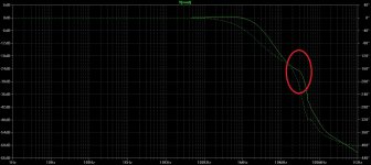
One question remains. Looking at the attached schematic and loopgain plot, why does the gain rise from 0.1Hz to a peak at around 4kHz? This does not happen if I place the probe at the base of the first VAS transistor. I wonder if you have seen plots of this shape before?
Any thoughts?
Thanks,
Ian
I've now implemented a 'homemade' Tian loopgain probe in pspice. The results correspond well with the now fixed Thompson Middlebrook'75 probe.
One question remains. Looking at the attached schematic and loopgain plot, why does the gain rise from 0.1Hz to a peak at around 4kHz? This does not happen if I place the probe at the base of the first VAS transistor. I wonder if you have seen plots of this shape before?
Any thoughts?
Thanks,
Ian
Attachments
Last edited:
Hi ihan,
Your circuit looks very good 😉
Why you place the Tian at that place?
You should put it connected to the first transistor's base, I think, after the dominant pole miller frequency compensation capacitor.
PS:
I have an instabillity in my VI limiter 😛
Best regards,
Daniel
Your circuit looks very good 😉
Why you place the Tian at that place?
You should put it connected to the first transistor's base, I think, after the dominant pole miller frequency compensation capacitor.
PS:
I have an instabillity in my VI limiter 😛
Best regards,
Daniel
Last edited:
Hi Daniel,
I placed it there because I get different low frequency results compared with placing the probe at the base of the first vas transistor. I don't understand why there is a difference, and I was hoping someone could explain why.
Attached are the results with the probe at the first VAS base.
Cheers,
Ian
Attachments
I've now implemented a 'homemade' Tian loopgain probe in pspice. The results correspond well with the now fixed Thompson Middlebrook'75 probe.
Nice to read that you were able to find the error in the Thompson implementation of Middlebrook 1975.
One question remains. Looking at the attached schematic and loopgain plot, why does the gain rise from 0.1Hz to a peak at around 4kHz? This does not happen if I place the probe at the base of the first VAS transistor...
Another error? Does this happen with your corrected T/M1975 circuit?
The traces should be identical when you place the probe there or at the base of the first transistor.
They match perfectly in LTspice, in fact I had to alter one just a bit to make sure I had two traces.
Best wishes
David
Hi ihan,
Plot the phase to see if you have sufficient phase margin at the 0dB point
😉
Best regards,
Daniel
Plot the phase to see if you have sufficient phase margin at the 0dB point
😉
Best regards,
Daniel
Hi David,
Yes, it happens with the uncorrected M75, the corrected M75, and my newly created (from scratch) Tian.
They all show a rising low frequency response when the probe is placed between the two transistors.
Thanks for your help.
Yes, it happens with the uncorrected M75, the corrected M75, and my newly created (from scratch) Tian.
They all show a rising low frequency response when the probe is placed between the two transistors.
Thanks for your help.
Hi David and ihan,
Sorry for interrupting your interesting conversation,
Could you help me here when you have time, now my amplifier seem to be stable, but another project I've, for a lower power headphones amp are with VAS stability problems
🙁
Best regards,
Daniel
Sorry for interrupting your interesting conversation,
Could you help me here when you have time, now my amplifier seem to be stable, but another project I've, for a lower power headphones amp are with VAS stability problems
🙁
Best regards,
Daniel
Attachments
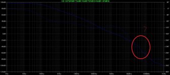
I've located the culprit - see attached schem and loopgain plot.
If I remove the VAS psu filter (22R & 2200uF in the VAS supply rail), all is well (with all 3 probes).
Next question for us to answer: Why does this filter change the response?
Thanks for the continued dialogue.
If I remove the VAS psu filter (22R & 2200uF in the VAS supply rail), all is well (with all 3 probes).
Next question for us to answer: Why does this filter change the response?
Thanks for the continued dialogue.
Attachments
Last edited:
Next question for us to answer: Why does this filter change the response?
Thanks for the continued dialogue.
It is presumably because with the VAS psu filter fitted, there is signal on the VAS psu node (its AC impedance is non-zero with the filter in place)?
I've located the culprit - see attached ...
If I remove the VAS psu filter (22R & 2200uF in the VAS supply rail), all is well
That makes sense. The time constant matches, that should have been a clue.
I did not test a simulation with a filter on the VAS, just a quick check with a V source on the rail.
As I said, I have seen such discrepancies in tests and suspect they reveal information about secondary effects.
This is the first one I have seen nailed down, very educational, thanks.
Best wishes
David
- Status
- Not open for further replies.
- Home
- Amplifiers
- Solid State
- Minor Loop Stability Analysis for dummies