Have you tried just changing the input transistor to a newer one? Might be all you need to do. Just noticed the .5v Vbe, are these germanium? Then not just a 1 transistor swap.
I stumbled upon an intresting circuit in the 02/10/11 issue of electronic design on page 100 with a diode in a similar situation.
Might be there just to bias the second transitor with out using an emitter resistor and losing VAS gain.
Yes,you may very well be right as I am not compleatly familar with the operation and design of the VAS stage yet.
I used silicon parts in the simulation and it came up with .564v Vbe on the first stage aswell. jer
I used silicon parts in the simulation and it came up with .564v Vbe on the first stage aswell. jer
Is the second stage Vbe also that low in the sim ( I think the post shows .5v also)? A little low but if the currents are low enough.... Are you using models for that particular transistor (where did you find it?) or a generic model?
I'm thinking of several changes. Lower noise transistors, more current on the first stage, and to deal with that, perhaps 2 or 3 diodes in series on the second stage, with more bypass capacitance for the bias network of the first stage. Finally, eliminating coupling cap at the output! Any thoughts?
More current means lower resistances means the transistor emitter resistance will become part of the gain equation which will decrease the gain and increase distortion. You will have to figure out at what point this effect becomes a problem.
It will also decrease the input impedance of the stage (dependant on the Hfe of the new transistor).
I was kind of thinking of an FET input if I could find one with enough gain. They can be tricky, as for a given type the gain can be all over the place, then there is the problem of noise- not all FETs are all that quiet! But they would allow me a higher input impedance, which is important since there are 35 tape heads in series at the input. Plus I have a bag full of IFN147s... otherwise I need to find quiet subs for the first two transistors and see if that has any effect. The problem is that even when new, this was a problem with the Mellotron circuit.It will also decrease the input impedance of the stage (dependant on the Hfe of the new transistor).
The 82K and 2.2M resistors probably should not be changed. I did replace them with precision devices (about 5 years ago); the gain of the circuit is fine and of course they are part of the tape EQ.
As far as the output goes, a single cap that is small enough seems to be all that is needed. They must have added the second one (which frankly does look like it was added as an afterthought, as it is just tacked on to the board) once the low frequency hump was discovered.
I was kind of thinking of an FET input if I could find one with enough gain. They can be tricky, as for a given type the gain can be all over the place
That goes for transistors too. And it also changes with temp. Thats why for circuits that you need to know the gain you set it with resistors, like in the present circuit, the first stage gain is very close to 470k/100ohms.
The dominant noise source for the entire cct will be the first stage. If I were you I would try the easiest thing first, swap just the input transistor with a new one ( maybe a BC560 or the like). I bet this will be all you need to do.
Sorry, it has taken me a while to respond as I have been learning some more things about circuit maker.
It does do noise but I haven't got it to work yet.
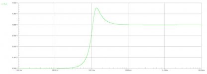
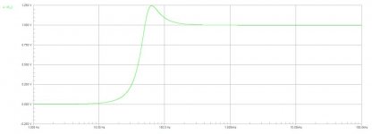
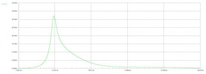
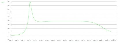
Here are the sims I have done so far and I hope they come out okay or else I will have to resize them again to repost.
Some of them are with some component value changes and I will have some comming hopful tomorrow.
The graphs are labeled with the changes.
I didn't know what transistor to use for the PNP so I tried many and they made little difference as to which one I used.
I also found the that changing the 82k resistor for changing did effect the frequency response a little but not enough to be alarmed about and I wil have those graphs tomorrow as well.
Enjoy. jer
It does do noise but I haven't got it to work yet.
Here are the sims I have done so far and I hope they come out okay or else I will have to resize them again to repost.
Some of them are with some component value changes and I will have some comming hopful tomorrow.
The graphs are labeled with the changes.
I didn't know what transistor to use for the PNP so I tried many and they made little difference as to which one I used.
I also found the that changing the 82k resistor for changing did effect the frequency response a little but not enough to be alarmed about and I wil have those graphs tomorrow as well.
Enjoy. jer
Attachments
-
 COLLECTOR OF Q3.jpg20.4 KB · Views: 141
 -
 EMITTER OF Q3.jpg24.7 KB · Views: 144
 -
 FR BASE OF Q3 C6 .022UF.jpg19 KB · Views: 149
 -
 FR BASE OF Q3 C6 .22UF.jpg19 KB · Views: 130
 -
 FR BASE OF Q3.jpg20.9 KB · Views: 123
 -
 NODE OF C2 AND C3.jpg24.8 KB · Views: 66
 -
 NODE OF R3 AND R4.jpg22.5 KB · Views: 72
 -
 OUTPUT R1 10K.jpg25.3 KB · Views: 69
 -
 OUTPUT R1 5K.jpg25.5 KB · Views: 75
 -
 OUTPUT R1 1K.jpg25.7 KB · Views: 82
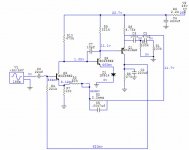
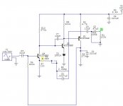
And the schematic.
I don't know why the scale is displaying Kv range.
I think it could be do to the high gain of the circuit.
Hopfully, I will figure it out.
I have been using this program since it first came out but there is alot that it does do that I haven't learned yet. jer
I don't know why the scale is displaying Kv range.
I think it could be do to the high gain of the circuit.
Hopfully, I will figure it out.
I have been using this program since it first came out but there is alot that it does do that I haven't learned yet. jer
Attachments
Last edited:
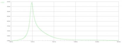
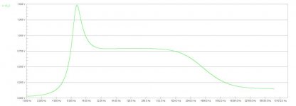
Sorry that they are not organized because I just wanted to get them posted.
The next ones will be better catagorized.
If there are no component change listed then the graph is as the original schematic as shown. jer
The next ones will be better catagorized.
If there are no component change listed then the graph is as the original schematic as shown. jer
You show a 100K resistor to ground between the first and second output coupling caps. It may well be reasonable since you are finding the low frequency bump, and that might be a logical place to put it. But there is no such resistor in the actual circuit.
The 100k resistor is there to serve as reference for circuit maker change this resistor to a 10megohm shows no diference freqeuny response.
Circuit Maker errors when it tries to process an unterminated capacitors.
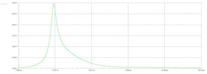
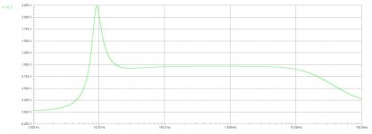
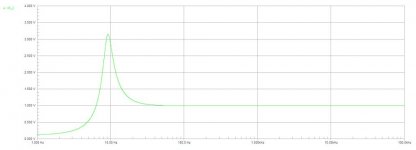
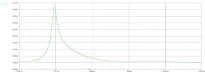
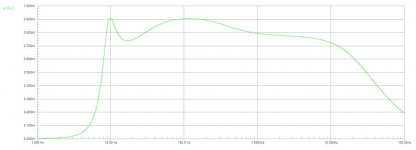
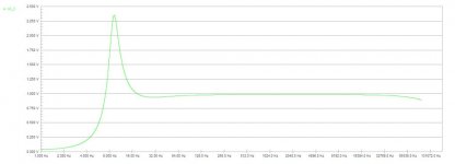
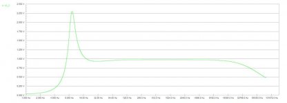
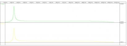
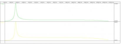
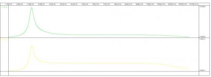
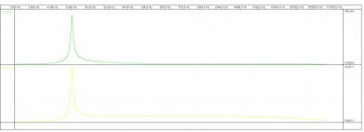
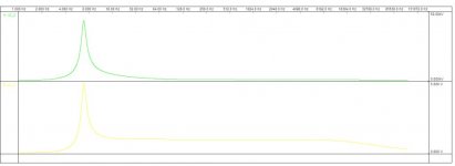
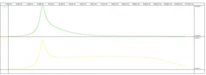
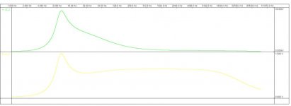
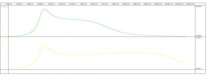
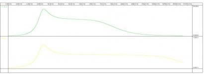
Here are the frequency response simulations of the effect of changing the gain of the circuit by changing the 82k resistor.
The samples were taken from the collector of Q3 the first transistor.
The low frequency hump is due to the value of the input capacitor and shifts up in frequency as the value is reduced. jer
P.S. There isn't a setting In Circuit Maker the show the graphs in db,sorry.
Circuit Maker errors when it tries to process an unterminated capacitors.
Here are the frequency response simulations of the effect of changing the gain of the circuit by changing the 82k resistor.
The samples were taken from the collector of Q3 the first transistor.
The low frequency hump is due to the value of the input capacitor and shifts up in frequency as the value is reduced. jer
P.S. There isn't a setting In Circuit Maker the show the graphs in db,sorry.
Attachments

Last edited:
I measured the volume control. Its 10K. Also I installed a jumper on the pcb to bypass the 1st of the two output coupling caps since the second cap predominates in the value of the two in series.
Shorting out the input has almost **no effect** on the noise! At present I am thinking an FET input with the same values in the source and drain circuits, but with the 221K bias resistor removed and instead a 50K resistor in parallel with the input. It might be at that point the input coupling cap could be eliminated.
Shorting out the input has almost **no effect** on the noise! At present I am thinking an FET input with the same values in the source and drain circuits, but with the 221K bias resistor removed and instead a 50K resistor in parallel with the input. It might be at that point the input coupling cap could be eliminated.
That circuit could be mocked up on a bread board very easily and it would be much easier to plug and play your parts configurations until you find a combination that works for you.
I will try some fets in the simulation,It doesn't have an MPF102 but it does have some other common ones such as the 2N5459 and BS170 just to name a few. jer
I will try some fets in the simulation,It doesn't have an MPF102 but it does have some other common ones such as the 2N5459 and BS170 just to name a few. jer
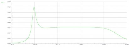
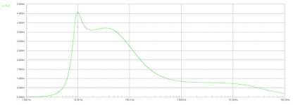
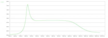
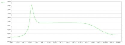
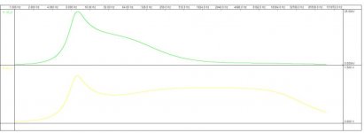
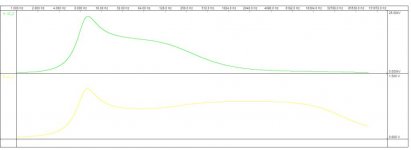
Yes, it does change the low frequency response, but it doesn't change the center frequency of the hump.
Only changing the input capacitor (22uf) does this.
I will do some plots of different values of capacitance values of the feedback capacitor taken from the output of the circuit. jer
Only changing the input capacitor (22uf) does this.
I will do some plots of different values of capacitance values of the feedback capacitor taken from the output of the circuit. jer
Here are the rest of them. jer
Attachments
-
 C5 .01 UF.jpg18.8 KB · Views: 68
 -
 C5 .022 UF.jpg19.1 KB · Views: 64
 -
 C5 .047 UF.jpg19.9 KB · Views: 72
 -
 C5 .0047 UF.jpg19.9 KB · Views: 57
 -
 C5 .0022 UF.jpg20.4 KB · Views: 67
 -
 C5 .001 UF.jpg20.5 KB · Views: 62
 -
 C5 470 PF.jpg20.6 KB · Views: 59
 -
 C5 220 PF.jpg20.5 KB · Views: 65
 -
 C5 100 PF.jpg20.4 KB · Views: 70
- Status
- Not open for further replies.
- Home
- Live Sound
- Instruments and Amps
- Mellotron preamp schematic