Well the OPA1656 certainly has some seriously impressive datasheet specs, especially for a very reasonable price.
There's no question that this could be designed with 5534s- AP did it, and the performance of even the ancient System One cannot be argued with. That said, it's very possible that 30 years of op-amp development can allow for a simpler design.
I'll have to think about the FET current limiter idea. I'm having a hard time visualizing it. I'm also going to see if AoE has a "recommended" solution for input current limiting on something like this- it really isn't all that unique of a design requirement.
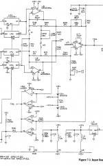
Okay, here's the current update. I presume this is the sort of depletion FET input circuit that was mentioned. The circuit added to the schematic is basically copy-and-pasted out of AoE, so I need to make some tweaks in order for it to suit this design. Sorry the symbols are for an enhancement FET, KiCad apparently doesn't have a depletion FET symbol in its library. In particular, the LND150 has an on resistance of 1000 ohms, so we've basically put a 3k resistor in series here- I'm thinking this can be improved. The CPC3982TTR from IXYS looks promising. Some of the bigger depletion FETs offer a much lower on resistance, however, they also feature capacitances that are about 1000 times higher.
I also changed out the clamping diodes with back-to-back zeners. I did this for a number of reasons. First, the other solution does allow a large signal to drive the input of the amplifier one diode drop past the rail. Second, as mentioned before it has the potential to affect the voltage rails. These zeners will need to be somewhat stout, though hopefully the FET current limiter mitigates this somewhat. Irritatingly, datasheets for zeners typically don't include capacitance values, which would be nice to know in this application.
The autoranger shows the LTC1967. The type of waveform where this will potentially become inaccurate is also the type of waveform that is rarely being measured by an audio analyzer, and for that type of waveform there is always manual ranging- something I have yet to draw into the schematic but which will absolutely be an option.
Attachments
I am currently looking at the FET based protection and have made some preliminary tests.
I would suggest to change the FET's to BSP129 from Infineon. They have an ON-resistance of around 6 ohm. And change the resistor to 200 ohm. This will give a total resistance of around 215 ohm and a maximum current of around 10 mA.
I would move the FET circuits to between the junction at C4/R67 and pin 7 of K4C (and the same for the other polarity). You don't need the protection when attenuating the input signal.
You should probably remove R23 and R24.
And use a better clamp circuit. I think that the zener diodes will generate a relatively high level of distortion.
To reduce the noise you could scale the feedback resistors around U3 and U4A.
I am currently looking at the FET based protection and have made some preliminary tests.
I would suggest to change the FET's to BSP129 from Infineon. They have an ON-resistance of around 6 ohm. And change the resistor to 200 ohm. This will give a total resistance of around 215 ohm and a maximum current of around 10 mA.
I would move the FET circuits to between the junction at C4/R67 and pin 7 of K4C (and the same for the other polarity). You don't need the protection when attenuating the input signal.
You should probably remove R23 and R24.
And use a better clamp circuit. I think that the zener diodes will generate a relatively high level of distortion.
To reduce the noise you could scale the feedback resistors around U3 and U4A.
I hadn't seen the BSP129- looks quite interesting. Input capacitance is a little high, though I doubt it will cause an issue, and the on resistance looks excellent.
Feedback resistors around U3 and U4A were chosen to try and find a balance between minimizing noise and minimizing excessive loading of U3A and U3B. The OPA1656 has decent load driving capability, but its distortion starts to rise significantly with loads below 2k.
As for the zener diodes, are you thinking in terms of non-linear capacitance?
Non-linear capacitance and leakage current as a function of the voltage (soft knee).
Remember that if you have a large source impedance or you use attenuation, even nano amps of leakage current variation will give a relatively large error. E.g. 1 nA and 10 kohm will give you an error of 10 uV. That is only 100 dB below 1 V.
Is the input capacitance of the FET's important? Once you start changing the gate-source voltage you are already in the clipping region. In normal operation there should be very little voltage across the FET's.
The FET input capacitance shouldn't matter except for very high frequency transients. I'm not too worried about that, however, since this isn't being used to measure mains power, for example.
I'll do some looking into the best solution for a clamping circuit.
I'll do some looking into the best solution for a clamping circuit.
I was thinking of something like this: http://ww1.microchip.com/downloads/en/DeviceDoc/DN2540 B060313.pdf with 400V breakdown and intended for off line service. I might try retrofitting into some of my analyzers. The input series resistance is the limitation on the noise floor given todays best opamps.
Input C modulation is a real limitation on distortion floor once the source impedance increases. 1 PPM distortion comes from a pretty small variation in input C and semiconductors all show significant CV aspects.
Input C modulation is a real limitation on distortion floor once the source impedance increases. 1 PPM distortion comes from a pretty small variation in input C and semiconductors all show significant CV aspects.
1N4148 spec shows something like 20 nA of leakage and about 4 pF of capacitance. Perhaps reconfiguring the zener clamp to have two zeners, each in series with a 1N4148, in parallel, if that makes sense.
Furthermore, perhaps with a bit of digging it may be possible to find a diode with lower leakage and lower capacitance than the 1N4148.
Furthermore, perhaps with a bit of digging it may be possible to find a diode with lower leakage and lower capacitance than the 1N4148.
I was thinking of something like this: http://ww1.microchip.com/downloads/en/DeviceDoc/DN2540 B060313.pdf with 400V breakdown and intended for off line service. I might try retrofitting into some of my analyzers. The input series resistance is the limitation on the noise floor given todays best opamps.
Input C modulation is a real limitation on distortion floor once the source impedance increases. 1 PPM distortion comes from a pretty small variation in input C and semiconductors all show significant CV aspects.
The DN2540 could also be an option although the ON resistance is a bit higher than for the BSP129.
If the input resistance is kept at around 215 ohm, the input amplifier could dominate the total noise unless the amplifier has a very low noise. With the OPA1656 a 215 ohm resistor will have little influence on the total noise.
When I wrote about input capacitance of the FET's I was thinking of the FET's in the protection circuit, not the FET's in the input amplifier. I agree that modulation of the input capacitance of the amplifier will lead to distortion when the source resistance is high. I know that TI has minimized the input C modulation on e.g. the OPA1642. I assume that they have done something similar in the OPA1656, but I haven't seen any info on that.
I was thinking of something like this: http://ww1.microchip.com/downloads/en/DeviceDoc/DN2540%20B060313.pdf with 400V breakdown and intended for off line service. I might try retrofitting into some of my analyzers. The input series resistance is the limitation on the noise floor given todays best opamps.
Input C modulation is a real limitation on distortion floor once the source impedance increases. 1 PPM distortion comes from a pretty small variation in input C and semiconductors all show significant CV aspects.
The DN2540 could also be an option although the ON resistance is a bit higher than for the BSP129.
If the input resistance is kept at around 215 ohm, the input amplifier could dominate the total noise unless the amplifier has a very low noise. With the OPA1656 a 215 ohm resistor will have little influence on the total noise.
When I wrote about input capacitance of the FET's I was thinking of the FET's in the protection circuit, not the FET's in the input amplifier. I agree that modulation of the input capacitance of the amplifier will lead to distortion when the source resistance is high. I know that TI has minimized the input C modulation on e.g. the OPA1642. I assume that they have done something similar in the OPA1656, but I haven't seen any info on that.
I was referring to the FETs in the protection circuit. A large input capacitance could potentially cause a problem with a very fast transient on the input, as it could lead to a large drop over R46/R47 and perhaps exceed the gate-source voltage rating of the FETs. That said, I'm not worried about it since the input filtering network will limit the rise time of any such transients to the point where it is a non-issue.
Attached is the idea I had for getting around the leakage and nonlinear capacitance of zeners, using a better diode in series. I think I can find something better than a 1N4148 to use in that position as well.\
I also moved the current limiting FETs as suggested- good call. That's exactly where the incandescent lamps are located in the System One. My hope is that they are a slightly more obtainable solution going into the future than a 60V incandescent lamp...
Attachments
Last edited:
How do you plan to introduce the hysteresis? I cannot imagine an autoranger having none, it could easily kill the relays, IMO. But I may be missing something, as is usually the case. Thanks.
I haven't quite figured that out yet- been mulling it over for the last few days without much success. Suggestions are welcome.
Hi H317,
Sketched below is one possible way to introduce hysteresis into the comparator thresholds. I’ve suggested independent bias divider strings as that makes it easier to tweak thresholds and hysteresis deltas without disrupting the parameters in other comparator sections.
My sketch also suggests a way to design out the diodes in the emitters of the relay drive transistors. (It also reduces comparator current draw a bit when relays are switched off.) Open collector outputs of the comparators will switch between -15V and about +0.7V (neglecting loading from the hysteresis feedback resistance).
An alternate design uses a 2N2007 MOSFET instead of bipolars. Comparator outputs switch between roughly +/- 15V (again neglecting loading from the hysteresis feedback resistance).
All this said, I like your mention of using a microcontroller (post 34) and suggest the concept in the final sketch for your consideration. It proposes a full-wave peak detector that would capture peak amplitude for presentation to the controller’s A/D. Software would manipulate the relays to raise sensitivity until an appropriate range has been reached. The peak detector would use a CMOS opamp for low droop and the Reset transistor allows the peak detector to be discharged as needed for continual monitoring. I think this approach might resolve issues of ripple suppression over a broad frequency range, obviate relay chatter, etc. Of course, everything always works perfectly in my imagination. 😉
One last thought is to incorporate a relay that would bypass the protection network at the final phase of challenging THD measurements. This feature would be engaged only at operator discretion (press to test?) when possible protection-network distortion needs to be ruled out; the feature would disengage automatically to minimize exposure to overload.
Good luck with your project!
Steve
Attachments
I thought this description of the Boonton input overrange circuit would be helpful. Especially since it uses LM339's. In principle you want an overrange trigger that is essentially instantaneous and a down ranging circuit that's slow to go downrange. 3 sets of comparators could handle the task. Overrange, above range and below range.
A simple up/down counter plus something like this could handle the ranging. 10 dB steps would be a better way to exploit the capabilities of a soundcard ADC.
I don't think you need to make any special bypass for ultra low distortion. The Boonton with opamp upgrades is already at about the limit of the Shibasoku 725's measurement floor. Which is below that of any ADC's I have tested.
Attachments
Sorry for the radio silence, things got excessively busy for a while.
From what it sounds like the Boonton uses the window detectors only for the 40 dB attenuator, and the rest are controlled by the CPU. Is this the case?
Here's one way I'm considering doing this. Two comparators, one senses over-range and the other senses other range. A little hysteresis is implemented to stop them from oscillating and confusing the microcontroller.
All the microcontroller nerds are going to cringe at this, but it's basically an Atmega328 programmed using the Arduino IDE. I did this for two reasons. First, my experience with microcontrollers is a bit limited. Second, this is supposed to be DIY-friendly.
Attachments
IMO there is nothing wrong with using arduino, if the design allows slightly lower performance due to the universal purpose of the libraries. Plus using one of the USB-enabled boards would give you a direct connection to PC, e.g. for reading current range and keeping dBV analyzer charts updated or for automated control.
Quite honestly I think the disadvantages of the Arduino won't show here since it really isn't being pushed at all. Power consumption is almost zero concern, and the microcontroller is really just being used to replace a bunch of 7400 series logic chips.
Readout of ranges will probably be done with a few LEDs. I don't see a huge advantage to anything else, really, although if people really want PC control over USB or RS232 then that could be implemented.
IMO, absolute level readouts is sort of optional, since most people probably have a decent true-RMS multimeter with sufficient bandwidth. It would be relatively straightforward to design a module with a trueRMS converter for one of the "ASP" expansion slots. The original goal of these "cards" was to allow easy and convenient switching between different notch filters and a distortion magnifier, but a level readout card could be done as well. It would need to be calibrated in-place.
What I meant was keeping the analyzer software aware of current range = current conversion dBFs => dBV. With that available the analyzer should rescale a chart when the range changes automatically.
Integrated analyzer combos SW+HW have this coded in. I am aware that the existing standalone software analyzers do not have any means of external control but maybe that could change if there were enough interest. A simple python script could provide the control.
Integrated analyzer combos SW+HW have this coded in. I am aware that the existing standalone software analyzers do not have any means of external control but maybe that could change if there were enough interest. A simple python script could provide the control.
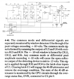
It occurred to me that it is worthwhile to sense common-mode voltage for the auto-ranging attenuator the way the Boonton does. That is now shown on the schematic.
I was a bit hesitant to add this because it does add a fair bit of complexity, and I struggle to come up with a situation where a an AC common-mode voltage of high enough magnitude to justify switching ranges will be present, but it only adds one chip to the board.
I was a bit hesitant to add this because it does add a fair bit of complexity, and I struggle to come up with a situation where a an AC common-mode voltage of high enough magnitude to justify switching ranges will be present, but it only adds one chip to the board.
Attachments
- Home
- Design & Build
- Equipment & Tools
- Measurement Interface for Sound Card