The basic layout of all CDPs in this series is the same, and it has several rather annerving flaws:
1) There are several ground routing errors.
In particular, the CD1020 has the middle wire of the power transformer windings for analog and digital power, connected internally inside the transformer, so this is where the analog and digital ground are connected... the first time. Sadly, they also connect at the PSU fulter caps, and then once more after the analog regulators.
The correction is to disconnect the midpoint connection of the analog PSU filter caps to the digital PSU V+ filter cap (this is done by removing a jumper on the board) and connect it via a wire directly to the transformer ground pin. Also, the connection of the midpoint of said analog PSU filter caps should be severed from the analog regulator ground. There is a parallel ground connection from there to the digital V+ filter cap, which should also be disconnected. The ground of the analog regulators again has a connection to the star ground point at the output connector where the actual analog and digital grounds connect. So, in all, there are 3 parallel connections as the board is routed, forming no less than two ground loops! I have not given speciffics on where to find this on the board layout as it is slightly different between CD43/53/63 and CD1010/1020.
2) The analog section of the DAC chip is powered from the digital power supply, and this is actually a double problem as there is a separate analog supply for the clock generator and the PWM outputs (these actually have several ground and power pins, for each channel). So:
2a) The clock power supply is derived from the DIGITAL power supply via a simple RC filter consisting of a 10 ohm resistor and caps to ground.
It should be noted here that any noise injected into the clock supply appears as jitter in the system, as the DAC clock is the reference clock for the whole player. Of course, the DAC clock is connected to the actual PWM DAC inside the chip, providing a direct jitter injection path.
The DAC datasheet clearly states that the quality of the clock power supply hugely affects the DAC performance, which is not a surprise considering this is a PWM DAC with only 13-position quantizing, running at 1.4112MHz PWM rate. It should be noted that due to it's low bit design, clock jitter performance is paramount. One look at the power supply for the clock circuit will show tens of mV of noise clearly correlated with the workings of the digital portion of the player and the servo circuits.
The correction is a two step approach. For starters, the clock power supply is ANALOG, not digital. The clock directly influences digital to analog conversion, and should be supplied from the analog supply.
Further, it should be as low noise as possible.
Fortunately, the current draw for this circuit is fairly constant so a simple shunt regulator can be used.
In my mod, a BF245B JFET is connected as a current source, and selected for a current of around 12mA. The R from the RC filter is removed and the current sourced from +12V analog, via the FET is fed to the clock power pin. The ceramic cap in parallel with the clock power is replaced by a chip cap under the board, and the mounting holes are used for two selected green LEDs in series, forming a shunt element with a knee voltage of around 4.1V.
Although the LED is not the ideal shunt element because it's knee is not as steep as say a zener or an integrated shunt regulator like the TL431 for instance - which is another way of saying that it's dynamic impedance is not as low - it has the great advantage of being extremely low noise. The electrolytic cap in parallel with the supply pins has also been changed to a Sanyo OSCON 1200uF/6.3V. Since the circuit itself only uses about 0.5mA of current, the cap leakage and shunt bias are amply covered by the JFET sourcing 12mA.
The improvement in the amount of injected noise is quite staggering - at least 40dB, and probably closer to 60dB, very difficult to measure because it is so small that all sorts of inductive effects generated in the probe wire greatly affect the reading.
It may also be possible to use a single dark blue LED, at least 3.6V is required for everything to function properly.
It is not needed to take special care with PSU sequencing for this as the slock is semi-static - the power only has to come up before the reset procedure for the DAC is finished (this takes a second or two so it's easily satisfied).
2b) Perhaps the most perplexing error - the power supply for the PWM DAC outputs is DIRECTLY connected tot he digital +5V power supply, with no filtering whatsoever - even though positions for RC filters are provided.
It should be noted that while the power supply rejection ratio of the PWM output is dependant on the actual calue they assume, it is never more that a measly 12dB! There are hundreds of mV peak noise in this power line and they are directly transfered to the DAC output. Although a lot of it is HF and gets filtered out by the analog stage, most of it is well within the audio band, and the PWM process further intermodulated it all both up and down the spectrum. This is why it can't be heared as correlated noise, but it adds a lot of 'haze' into any complex recording, especially orchestral pieces.
This is perhaps the most obvious place to improve any of the CDPs from that series!
THe correction is similar to the one used for the clock supply. In this case, however, two shunt regulators are assembled, one for each channel. Again, BF245B selected for about 12mA Idss form current sources, and again they are cupplied from the analog +12V.
THis time, three red LEDs are selected to form a shunt element with a knee voltage at about 5V. The tricky part is, you need to select them, so that the shunts for the left and right channel are as close to each other in voltage. Also, a lower voltage translated into a lower output from the DAC, and we want as close to nominal as possible. In the end two dark red and one regular red LED in series, fored 5.05V shunts.
The bypassing for these is a bit more involved than that for the clock shunt, because of the PCB layout, which is very long-line and not very optimal for a circuit operating at those frequencies.
Chip caps are used right at the DAC pins (4 in all), 1nF NPO. This keeps most of the RF energy formed by imperfect swtiching, in a loop inside the DAC. 1200uF oscons in parallel with 0.22uF non-inductive foils are used instead of the original similar parts. The layout uses two ceramics in parallel, one was replaced by the foil cap, the other by the shunt element.
IMPORTANT! This power supply line requires attention to power-up and power-down sequencing or the DAC chip may be damaged (read: latch up and literally explode!).
This is actually easy to do electrically but a bit difficult mechanically due to PCB layout - it has to be done on the solder side of the board. Each PWM V+ line must be connected to the digital +5V power pin on the DAC via two anti-parralel connected diodes (I used regular 1N4001). This ensures that the difference between analog and digital power is never more than 0.7V, and insures proper power sequencing.
Again, the reduction in injected noise is even better than that of the clock supply, because the PWM output supply in the original has about 10x more noise to begin with.
It should be noted that the PWM outputs do not use the full quantization (13 positions) for useful audio signal, a fair number is used for the noise shaping and dithering. Because of this the DAC actually generates about 1.4V RMS of useful differential output signal at full scale, a fact that the datasheet hides about as well as a snake would hide legs...
A couple of quick (I hope) questions.
(I fired this off before reading the detailed posts above, which have been helpful, if a little over my head. So my questions still stand, thanks, especially in relation to the SAA7323 clock supplies)
I have replaced the series resistors on the 5V supply lines to the digital chips with 470uH/2.5R inductors and two ferrite beads. I want to install separate regulators (analogue and digital) for each digital chip, fed by a new PSU.
1. Are the inductors with beads still necessary if I install the regs, or do I remove them when the regs are installed?
2. I have a spare 9 Volt, 10VA toroidal. Is the 10VA rating okay for this application?
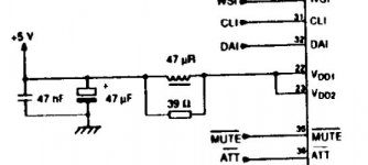
And a more general question that might be a little "off thread." I have a Rotel RCD965BX which uses the SAA7323 bitstream DAC. When I look at the +5V digital supply on the data sheet, I see that pin 22 is VDD1 "+5V supply for the digital section" and pin 23 is VDD2 "+5V for the crystal oscillator."
Both pins are tied together and decoupled with 47uF elco and & .047 ceramic, then a 47uH choke and 39R resister in parallel. (diagram attached)
This arrangement is quite different from the decoupling wisdom on this thread. I am wondering whether I should remove these parts and install a 470uH/2.5R choke with two ferrites beads, then either a 100uF or 220uF Os-con, and then a .1uF X7R cap from the pins to ground. I have these on hand.
Would this be an improvement, do you think? I could also give these pins their own regulator.
Cheers,
(I fired this off before reading the detailed posts above, which have been helpful, if a little over my head. So my questions still stand, thanks, especially in relation to the SAA7323 clock supplies)
I have replaced the series resistors on the 5V supply lines to the digital chips with 470uH/2.5R inductors and two ferrite beads. I want to install separate regulators (analogue and digital) for each digital chip, fed by a new PSU.
1. Are the inductors with beads still necessary if I install the regs, or do I remove them when the regs are installed?
2. I have a spare 9 Volt, 10VA toroidal. Is the 10VA rating okay for this application?
And a more general question that might be a little "off thread." I have a Rotel RCD965BX which uses the SAA7323 bitstream DAC. When I look at the +5V digital supply on the data sheet, I see that pin 22 is VDD1 "+5V supply for the digital section" and pin 23 is VDD2 "+5V for the crystal oscillator."
Both pins are tied together and decoupled with 47uF elco and & .047 ceramic, then a 47uH choke and 39R resister in parallel. (diagram attached)
This arrangement is quite different from the decoupling wisdom on this thread. I am wondering whether I should remove these parts and install a 470uH/2.5R choke with two ferrites beads, then either a 100uF or 220uF Os-con, and then a .1uF X7R cap from the pins to ground. I have these on hand.
Would this be an improvement, do you think? I could also give these pins their own regulator.
Cheers,
Attachments
Hi ilizim,
three great great great postings !
very interesting....
Would you please explain why the clock power should be supply by the analog supply ? ( power transformer windings for analog ? )
100%, low noise is very important,
but because of the grounding the windings for digital power may be better ?
Regards
three great great great postings !
very interesting....
... the clock power supply is ANALOG, not digital. ...., and should be supplied from the analog supply.
Would you please explain why the clock power should be supply by the analog supply ? ( power transformer windings for analog ? )
The clock directly influences digital to analog conversion, ...
Further, it should be as low noise as possible.
100%, low noise is very important,
but because of the grounding the windings for digital power may be better ?
Regards
Hiilimzn said:Perhaps the most perplexing error - the power supply for the PWM DAC outputs is DIRECTLY connected tot he digital +5V power supply, with no filtering whatsoever - even though positions for RC filters are provided.
IMPORTANT! This power supply line requires attention to power-up and power-down sequencing or the DAC chip may be damaged (read: latch up and literally explode!).
This is actually easy to do electrically but a bit difficult mechanically due to PCB layout - it has to be done on the solder side of the board. Each PWM V+ line must be connected to the digital +5V power pin on the DAC via two anti-parralel connected diodes (I used regular 1N4001). This ensures that the difference between analog and digital power is never more than 0.7V, and insures proper power sequencing.
Your post denotes a deep knowledge of this kind of player.
Of course your info is too technical for some of us to grasp and I am having some trouble translating it to practical mods.
I have been modding my CDP following closely the info in this thread and already have 5 (five) separated TX and PSU´s, one for Servo, one for DAC, one for analog output stage, one for the clocks and I kept the stock one for the micro controler, display, decoder and HF amp.
I never had any problems on power up but also this is the first time I read about dac explosions.
I am very worried about this possibility as my player represents more than 2 years work and a considerable investment.
Would you please explain the diode setup based on a CD53 layout ?
Best regards
Ricardo
mm2 said:Hi ilimzn,
...
Would you please explain why the clock power should be supply by the analog supply ? ( power transformer windings for analog ? )
...
100%, low noise is very important,
but because of the grounding the windings for digital power may be better ?
Regards
Basically, it has to do with the fact that in the digital domain, time is a conceptual cathegory. The digital circuits will give exactly the same result out of the sam input regardless of clock frequency or jitter, as long as it is kept between the minimum and maximum frequency specified by the chip architecture, and this is actually a very wide range. The trick to it is that the timing part is 'concentrated' in the idea of a common clock signal, whose frequency is implicit. Consider that you could just as well read CDs with a 48k or 16k, or 0k sampling rate (like when it's sitting on a shelf...), and they wouldn't know it, what the data represents does not change.
It follows that 'time' actually becomes a variable at the point where the digital representation of analog values, becomes an actual analog value. This is because unlike a 'perfect' DAC, an actual DAC output value is not just a current or voltage proportional to the digital value of the sample, but it is a voltage/current integrated over time, the time being the length of the sample. This is because any kind of low pass filtering (even if it comes down to mechanical filtering of an amplified signal from a non-os DAC inside a speaker) has integrating characteristics. As a simplification, you can think of the DAC output value being voltage/current proportional to digital sample representation, times the length of one sample. As such, it represents a multiplication of two ANALOG values.
In practical terms, if you supply the digital parts of the DAC with a relatively unclean power supply, nothing much special will happen until the supply becomes so unclean that the digital circuitry stops functioning, i.e. skips clocks. The data it generates is re-clocked in the DAC output stage, so as long as the data for the next sample meets the set-up time for the PWM output latches, it will be successfully re-clocked and any jitter will be completely removed. So, depending on what part of the digital circuit we are looking at, the power supply could impart several tens to several hundreds of ns of jitter with no consequence at all to the DAC output.
However, the DAC PWM output stage must be supplied with an analog power supply, because in this particular NPC DAC it is also the 'reference voltage' for the DAC.
The PWM output latches is where the actual DA conversion takes place - and if you look at the datasheet, you will notice in the chip block diagram that there is a separate buffer from the clock circuit to the PWM output, to get a clean clock to the PWM latches, and it is supplied power from the clock power and ground pins.
The ideal solution would be to power the clock separately, with a PSU which is treated as analog - because any noise and perturbation in the power supply will be transformed into jitter, or, a variation in sample length - and directly affect the analog output (but not the digital - hence clock supply has to be 'analog'). What actually happens is that the variations in power supply voltage change the steepness of the clock output signal edges. Because the treshold voltage of the clock input of the PWM latch is fixed (this is the voltage at which the input is considered to turn from one logic state to another, in simplified terms), if the actual signal changes, the point where it's voltage is equal to the treshold voltage, also changes, it moves back or forth in time - this is how jitter is created.
In this particular DAC, all the power and ground pins are separated, so either a difference in the power or ground line potentials between PWM output and colcok circuit will end up being converted to jitter. Because there is no separate clock supply and ground, we have to use the next logical solution, which is to use a common ground for PWM out and clock, and derive both power supplies from the analog power supply. Although this power supply is also used by the output stage, it is not nearly as heavily polluted by noise correlated with the clock rate or the servo clock rate, which would result in a kind of jitter recirculation mechanism (similar to what you get in amps, recirculation of the harmonics the amp generates back to the input via the power supply).
Again, in practical terms, it has to do with the way the actual grond lines are connected under the DAC (I'm quite sorry now that I have not taken pics of the solder side of the PCB - it is slightly different on the CD101/1020 but not much).
As for the power transformer ground, this has no bearing on the issue, as the ground pin is common for both analog and digital. You have to remember that it is possible (and indeed preferable, and even done on these players, if you sort out the multiple grounding PCB routing errors) to return a ground line for the regulators of the various power supplies, from the point that we consider a ground reference, so that the regulators regulate out the difference between the reference point and actual power supply ground. You must remember that this is never the same as real life ground has an impedance and voltage drops all over it. All too often we assume it acts like some kind of superconductor, only because someone put a ground symbol in the schematic - in the real world, you have to route it carefully and count on the various voltage drops in it just like any other supply line. For a simple 'exercise' you might want to use a scope, put the ground reference clip onto the output connectors of the CDP, and the tip of the probe to the transformer ground pin. You may be surprised at the amplitude and waveforms you get!
Hi Ray6h5c said:
Gain of the discrete stage is reduced slightly to compensate for higher filter output. The gain of the entire circuit remains about the same; the 820 ohm goes hand-in-hand with the different values in the filter (values between brackets, see discrete PDF).
Just to be sure I decided to power the DOS with my bench psu (+-15v regulated).
Now I am reading 10.5v before the output cap.
In your pdf, I read a value 6.5v in that position.
Is this an issue ?
note:
The DOS is powered but without any input signal.
Regards
Ricardo
Hy,
the NPC DAC has three different ground pins: analog, digital, clock.
In the datasheet you can't see how they are internaly connected.
once I have cuted the common ground, and i could messure resitance between clock gnd and analog gnd.
because of this, my solution was to reconnect the clock and digital gnd ( like before )
and to connect the analog gnd to the gnd of the RCA socket.
( digital/clock gnd and analog gnd are now only connected by the power transformer )
I added three separate low noise regulators for analog, digital, clock.
( digital and clock from one power transformer winding,
and analog from the other one )
I hope now, noise and current from clock/digital should modulate the analog signal less than before ?
What do you think ?
If clock and analog gnd are connected
or the analog power transformer winding is used for both regulators
( clock and analog ) like you suggested,
I would fear that this leads to more noise and jitter ?
I agree analog should have the best low noise regulators ( 7805 is not okay )
clock should have the best or second best 😉 ( 7805 is not okay )
digital is unpretentious ( 7805 is okay )
Regards
the NPC DAC has three different ground pins: analog, digital, clock.
In the datasheet you can't see how they are internaly connected.
once I have cuted the common ground, and i could messure resitance between clock gnd and analog gnd.
You must remember that this is never the same as real life ground has an impedance and voltage drops all over it.
because of this, my solution was to reconnect the clock and digital gnd ( like before )
and to connect the analog gnd to the gnd of the RCA socket.
( digital/clock gnd and analog gnd are now only connected by the power transformer )
I added three separate low noise regulators for analog, digital, clock.
( digital and clock from one power transformer winding,
and analog from the other one )
I hope now, noise and current from clock/digital should modulate the analog signal less than before ?
What do you think ?
If clock and analog gnd are connected
or the analog power transformer winding is used for both regulators
( clock and analog ) like you suggested,
I would fear that this leads to more noise and jitter ?
I agree analog should have the best low noise regulators ( 7805 is not okay )
clock should have the best or second best 😉 ( 7805 is not okay )
digital is unpretentious ( 7805 is okay )
Regards
I agree.mm2 said:
I agree analog should have the best low noise regulators ( 7805 is not okay )
clock should have the best or second best 😉 ( 7805 is not okay )
digital is unpretentious ( 7805 is okay )
Nevertheless, changing from 7805 to LM340AT is a great improvement.
mm2 said:
the NPC DAC has three different ground pins: analog, digital, clock.
In the datasheet you can't see how they are internaly connected.
once I have cuted the common ground, and i could messure resitance between clock gnd and analog gnd.
This is because they are not internally connected except by chip parasitic structures, and one of them (unfortunately which one is not specified) is usually connected to the substrate. The chip should never be operated with any great difference in voltage between the ground pins. Normally in chip processes parasitic structures form transistors and SCRs, with treshold voltages from about 0.5 to about 1V. These should never be treiggered or the chip may (usually WILL) be damaged, so less than 0.5V difference between ground pins.
HOWEVER - even if it is within operational limits for the chip, this difference may be detrimental to chip operational specs, although the chip will not malfunction. For instance, any (noise) voltage between analog and clock ground has exactly the same effect as that same (noise) voltage on the clock or analog power supply line.
because of this, my solution was to reconnect the clock and digital gnd ( like before )
and to connect the analog gnd to the gnd of the RCA socket.
( digital/clock gnd and analog gnd are now only connected by the power transformer )
Actually, the analog and clock ground should be locally connected, and the digital and (common) analog ground connected at some other point.
In theory, ALL of these should ONLY connect at the DAC, but if you look at the PCB routing, this is not so - starting with a common ground connection for digital and analog supply windings in the transformer. I will try to put up a few schematics in the coming week to illustrate how it should be done (or rather, how it should be modified).
I added three separate low noise regulators for analog, digital, clock.
(digital and clock from one power transformer winding,
and analog from the other one )
As I said, the clock should be treated as an analog signal - because the clock generator circuit transforms clock power supply noise into jitter (time domain noise), which in turn the DAC transforms into noise at the output. I would supply the clock generator from an extra winding of the analog power transformer.
Even so, if it is supplied from an extra winding of the digital power transformer (assuming no common pins for the windings), a good regulator will greatly attenuate any noise transferred through the transformer from the digital power supply. In particular, the ground references for the regulators must be properly chosen, or additional local filtering must be employed nect to the DAC. Basically, what this means is that the regulators have a return ground from the point where the actual voltage they regulate is used - basically a form of load sensing/kelvin connection.
I hope now, noise and current from clock/digital should modulate the analog signal less than before ?
What do you think ?
If clock and analog gnd are connected
or the analog power transformer winding is used for both regulators
( clock and analog ) like you suggested,
I would fear that this leads to more noise and jitter ?
The way you described it, even if the regulation was perfectly noiseless, I don't think it will reduce noise coupling because you have a log run of wire all over the player connecting clock and analog+digital ground. Measuring with a scope should tell you everything - just easure the voltage between the two grounds and see for yourself.
Regarding using the analog supply for both clock and analog, see the lengthy explanation why the clock signal is ANALOG not digital in nature - it only gets to be 'digital' once it is shaped, divided down and used by the digital circuitry. Keep in mind that the clock signal is inherently mixed into the analog output on any DAC, this you can't avoid, it's the way the DAC works. So, even if your analog power line is slightly contaminated by the clock signal, you won't actually get additional jitter - the contamination has the exact same jitter as the clock!
Contrary to this, signlas generated by the player logic, CPU, servos ets may be driven by this clock or synched to it, but they have no correlation to the output signal, so they represent a form of noise. Unfortunately, they may have correlation to themselves, i.e. the noise is not random, but contains 'tones' or periodic signals. In either case, this is why you want to avoid contamination of either clock or analog power by any digital signal.
As can be seen on the internal schematic of the chip in the datasheet, the clock circuit is a simple oscillator and it's output is internally divided between two buffers, one for the digital portion of the DAC, one for the analog portion.
Because it's a PWM DAC, the 'analog' portion is actually a latch, which is used to re-clock the PWM data from the digital portion, to remove jitter generated by the complex digital circuitry. It is essential that the analog and clock grounds are actually connected, i.e. the difference is as close to 0V AC. Again, I have to repeat here - 'ground' is a conceptual thing. In reality, if you inject noise into the power supply line, it is exactly as if you inject it between the two grounds, if the Vcc voltage stays the same but GND varies, it is exactly the same as if the Vcc voltage varies but ground stays the same - you just change your point of reference, but the chip does not know that, it's a conceptual thing.
Again, why do analog and clock grounds have to be connected as close as possible on the chip itself? Because the reference for the clock INPUT of the analog stage is the analog ground, and the reference for the clock OUTPUT from the clock generator is the clock ground. If there is any difference in voltage here, the clock generated by the clock generator looks to the clock input of the analog stage as if it is moving up and down together with the noise signal - i.e. the noise is directly injected into the clock signal.
This will not be very detrimental for the digital circuits - it will work just fine as long as the injected noise is not so high as to approach the treshold voltage of the digital circuits, which would cause clock skipping. This is all possible because the end result of the digital process is reclocked in the analog output latch. Because of this, if a ground has to be disconnected from the other two grounds on the DAC, it has to be the digital ground.
Also, the ground references for the analog and clock power supply have to be connected to the ground connection of clock and analog ground, or the regulators will regulate with a wrong reference, injecting any difference into the power line.
This is the trick behind improving the analog regulator. Instead of using the local ground (which also has a loop in it!) for the 7812/7912, a separate ground is returned from the analog star ground, on the output connector. This largely takes care of the problem of the common analog and digital winding ground on the transformer.
I agree analog should have the best low noise regulators ( 7805 is not okay )
clock should have the best or second best 😉 ( 7805 is not okay)
digital is unpretentious ( 7805 is okay )
Regards
Actually, because it's a PWM DAC, the quality of the clock regulation can only be marginally worse than that of the analog one. How much is very difficult to measure (and you can really only measure it), and has to do with the power supply voltage variation, vs clock edge position variation of the clock circuit.
I do agree that 78xx are very inadequate here, but they can be perfectly fine as pre-regulators. For instance, I have not changed the 7812 and 7912 regulators for the analog stages because these voltages are either additionally filtered by RC filters for each OP-amp package, or post-regulated, in the case of my mod, by shunt regulators, to form the analog and clock power for the DAC.
And yes, I did change the 7805 original for a LM340T5, mostly because the original isolated package isn't as good in transferring heat, making the regulator run much hotter internally. I also used a better heatsink.
All power supplies and servo decoupling was beefed up (something to write about in the next post 🙂 ), but the analog regulators (7812, 7912) remain. The current drain after the mod is not that much bigger, about 60-70mA depending on the OP-amps chosen, so they stayed. It may be possible to replace them with low drop 15V regulators as some OPamps do show performance improvement at higher supply voltages - but then, others show unwanted thermal effects 🙁
I don't think it will reduce noise coupling because you have a long run of wire all over the player connecting clock and analog+digital ground.
...
So, even if your analog power line is slightly contaminated by the clock signal, you won't actually get additional jitter
...
if you inject noise into the power supply line, it is exactly as if you inject it between the two grounds, if the Vcc voltage stays the same but GND varies, it is exactly the same as if the Vcc voltage varies but ground stays the same - you just change your point of reference, but the chip does not know that, it's a conceptual thing.
...
Also, the ground references for the analog and clock power supply have to be connected to the ground connection of clock and analog ground, or the regulators will regulate with a wrong reference, injecting any difference into the power line
Yes, the point of reference is very important, but where ist this point of reference ? I think there are many :-(
In the original player the point of reference for the analog signal is near the RCA Sockets. But this point is far away from the DAC,
so there is a long run of wire to the DAC and the connection between clock and analog, which is the point of reference for the DAC.
This reduces jitter like you explained, but the current from clock and analog uses the same long ground wire. This current noise you will find at the RCA socket :-(
This is the trick behind improving the analog regulator. Instead of using the local ground (which also has a loop in it!) for the 7812/7912, a separate ground is returned from the analog star ground, on the output connector. This largely takes care of the problem of the common analog and digital winding ground on the transformer.
Again, where is the best point ?
Should the sense of the regulator be connected to ground near the DAC
( to reduce jitter noise ) or near the RCA socket ( to reduce current noise ) ?
I will try to put up a few schematics in the coming week to illustrate how it should be done (or rather, how it should be modified).
would be great, I'm looking forward to this
Regards
The last few posts have been very informative.
However I think the question in my post was lost in the middle of them. It was about DAC supply issues for another bitstream player the Rotel RCD965BX. I was hoping that the gurus here might be able to help, even though it might be a little "off thread."
The RCD965 uses the SAA7323 bitstream DAC. When I look at the +5V digital supply on the data sheet, I see that pin 22 is VDD1 "+5V supply for the digital section" and pin 23 is VDD2 "+5V for the crystal oscillator."
Both pins are tied together and decoupled with 47uF elco and & .047 ceramic, then a 47uH choke and 39R resister in parallel. (diagram attached)
This arrangement is quite different from the decoupling wisdom on this thread. I am wondering whether I should remove these parts and install a 470uH/2.5R choke with two ferrites beads, then either a 100uF or 220uF Os-con, and then a .1uF X7R cap from the pins to ground. I have these on hand.
Would this bring an improvement, do you think? I also want to give these pins their own regulator supplied from a separate transformer.
Cheers,
Joe
RCruz said:I notice the filter caps get warm to the touch..... BG forming
That's not good... are you sure you're not overloading them? They don't seem to be near a warm voltage regulator.
Ray
jnewbold said:...
Both pins are tied together and decoupled with 47uF elco and & .047 ceramic, then a 47uH choke and 39R resister in parallel. (diagram attached)
This arrangement is quite different from the decoupling wisdom on this thread. I am wondering whether I should remove these parts and install a 470uH/2.5R choke with two ferrites beads, then either a 100uF or 220uF Os-con, and then a .1uF X7R cap from the pins to ground. I have these on hand.
Would this bring an improvement, do you think? I also want to give these pins their own regulator supplied from a separate transformer.
Cheers,
Joe
Hi Joe,
I would separate the pins and give them each an OsCon and an inductor to +5V, and see what it does. Pin 23 probably supplies the internal inverters, and some extra decoupling reduces noise in the other power line. If you use a small 470uH...1mH inductor that has some DC resistance (like the 1mH/10R from Epcos), you don't have to use the parallel resistor.
Regards,
Ray
RCruz said:Testing
I notice the filter caps get warm to the touch..... BG forming
Do you mean the Black Gates are getting warm? Are they still the 470uF 16v ones?
If so, then they're getting warm due to running them at 15v. Have your 220uF 35v ZA's not arrived yet?
Lee.
Hi Ray6h5c said:
That's not good... are you sure you're not overloading them? They don't seem to be near a warm voltage regulator.
The caps are not near the sregs.
I also consider the heat strange.
Hi LeeThomo said:
Do you mean the Black Gates are getting warm? Are they still the 470uF 16v ones?
If so, then they're getting warm due to running them at 15v. Have your 220uF 35v ZA's not arrived yet?
I finished assembling the DOS before the ZA´s came.
I am using 220uF 25v BG FK I had in stock for another project.
They do get slightly warm to the touch (this is the first time I experience this with a cap)
The voltage is correctly set to +-15v and the caps are correctly polarized.

What other measurements can I do without any signal in the DOS input ?
Note:
Resistor R11 is getting too hot to touch....

Hope there is no damage.
Ricardo
Just found the heat source......6h5c said:
That's not good... are you sure you're not overloading them? They don't seem to be near a warm voltage regulator.
R11 is getting very hot
🙁It's probably the heat from R11 leaking away through the caps / heating them up?
R11 is dissipating about 0.36W. It is 1k8, right? And if i'm correct, there's about 25.5V across it in your situation? If this is the case, then it's normal for a 2W resistor to get too hot to touch. Humans can only barely hold on to 55 - 60*C 😀.
If you like, you can adjust R11 for the higher +/-15V supply voltage, just use a 2k2 or 2k4 instead of 1k8.
Ray
Yes to every question.6h5c said:It's probably the heat from R11 leaking away through the caps / heating them up?
R11 is dissipating about 0.36W. It is 1k8, right? And if i'm correct, there's about 25.5V across it in your situation? If this is the case, then it's normal for a 2W resistor to get too hot to touch. Humans can only barely hold on to 55 - 60*C 😀.
If you like, you can adjust R11 for the higher +/-15V supply voltage, just use a 2k2 or 2k4 instead of 1k8.
25v - 1k8 - 60ºC
It seems I am quite sensitive to hot temperatures
😀
It has been working for several hours and the temp keeps steady.. Hope the other components are not affected by the heat.
Maybe I should try a 2k2 instead.
What are the implications of this modification in your schematic ?
Ricardo
- Home
- Source & Line
- Digital Source
- Marantz CD63 & CD67 mods list