These are just random examples to help XRK971 to figure out how to use the topology and understand its limitations, I am not trying to design something specific or arrive at an optimum.
I think he now has enough information to get started, and if he hasn't, he can always come back and ask for further clarifications
I think he now has enough information to get started, and if he hasn't, he can always come back and ask for further clarifications
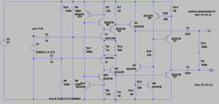
I have simulated a dozen+ phase splitters and it's very hard to beat a modern op-amp for that purpose. But if you must have a discrete circuit then consider the attached. Note that it will provide over 10Vrms and less than 0.001%THD. This does not attempt to combine both phases because that always compromises output level, precision, THD, and bad clipping behavior. As shown, the output transistors are over heated so a larger part or a lower supply voltage is recommended. A 24V supply will still give you 20VPP.
Attachments
Last edited:
Yes, I mentioned the possibility of using CFP's amongst others. Many more tweaks are possible, but I don't think it is worth reviewing them all. Concertina has limitations, as it has no options GNFB and to overcome them you need error-corrections schemes, preferably more elaborate than just diodes in the collectosr loadThis is a bit better at just under 0.08%.
A concertina is a negative-feedback transconductance amplifier with a resistor connected to its output. You can put as many stages as you like in the transconductance amplifier, you don't have to stop at one or two.
The classical concertina is, but the version I proposed has a transconductance-defining resistance distinct from the loadA concertina is a negative-feedback transconductance amplifier with a resistor connected to its output
You are free to stretch the definition as much as you like, and this would be the ultimate concertina, but I don't think many people would name it that way:You can put as many stages as you like in the transconductance amplifier, you don't have to stop at one or two.
Even this ultimate version, which can be made distortion-free provided the loop gain is high enough suffers from loads interaction. It could certainly be freed from that constraint, but it would need even more hardware, and people interested in concertina-type circuits are probably interested in simple, minimal active devices count options rather than complex, elaborate solutions (which can do the job, for sure).
I just wanted to show a simple example of eliminating a fundamental limitation of the basic concertina without exploding the BOM, not enter a lengthy controversy
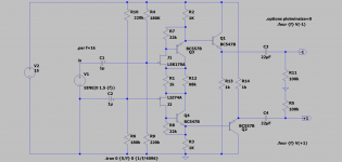
If you like the Concertina circuit, this may be as good as it gets. I have added EF buffers so that the loads have minimal effect. Using JFETs with separate bias dividers, the input impedance is about 100k. Using JFETs and setting the spice options, the THD starts to look respectable. Clipping is clean but not perfectly symmetric, but only a bit more than 3VPP. The 68K trim resistor adjust the gain very close to unity.
Attachments
A related issue hinted to by JonSnell's post #7 is the ~floating behavior of the two outputs. Do you want the output to behave like a floating transformer? The circuit Jon shows does this and it can reduce common mode noise, but my experience is that it is more trouble than it's worth because it can push the outputs into common mode clipping or instabilities. One benefit is that if one output is grounded, the full amplitude appears on the other output. Perhaps the ideal would be a floating output with a load center tap connected to ground.
It does improve the "+1" output significantly, but not so much the other. I don't have a good idea why. In any case, that was the side that needed improvement.Does it get any better when you replace R7, R8, R13 and R14 with current sources?
Attachments
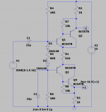
Elvee asked me to post a schematic of a differential pair with distortion compensation in the collector resistors. This is it:

This is for a gain of two, that is, signal voltage between E and D twice as large as the signal voltage between A and B. For larger gains, the collector resistors and the numbers of diode-connected transistors scale up proportionally. Like before, a non-ideal diode with an emission coefficient n of 1.752 can replace 1.752 diode-connected transistors, albeit at the expense of accuracy. The input signal is to be connected between A and B while D and E are the outputs.
There is one snatch that I hadn't thought about until Elvee triggered me: the circuit produces a distorted common-mode signal. Depending on the application, that can either be a disaster or irrelevant. It doesn't matter when whatever is driven by the output has a good common-mode rejection.
The voltage between the supply and D is an amplified copy of the voltage between A and C, and the voltage between the supply and E is an amplified copy of the voltage between B and C. The voltage between A and C minus the voltage between B and C is the input signal, so the voltage between E and D is just the amplified input signal. So far, so good.
However, when you look at each output individually, the distortion compensation doesn't work. It's only the differential voltage between the outputs that gets linearized.
Last edited:
Thanks.
Yes: here is the test:

And this is the complete test log:
Fourier components of V(1)
DC component:10.0062
Harmonic Frequency Fourier Normalized Phase Normalized
Number [Hz] Component Component [degree] Phase [deg]
1 1.000e+03 9.672e-01 1.000e+00 180.00° 0.00°
2 2.000e+03 5.404e-05 5.587e-05 -90.22° -270.21°
3 3.000e+03 5.860e-04 6.058e-04 -179.98° -359.97°
4 4.000e+03 8.191e-08 8.469e-08 -26.68° -206.68°
5 5.000e+03 2.246e-05 2.322e-05 0.02° -179.98°
6 6.000e+03 2.546e-08 2.632e-08 -45.16° -225.16°
7 7.000e+03 1.032e-06 1.067e-06 -179.35° -359.35°
8 8.000e+03 1.650e-08 1.706e-08 132.56° -47.44°
9 9.000e+03 4.457e-08 4.608e-08 5.27° -174.73°
Total Harmonic Distortion: 0.060885%(0.060872%)
N-Period=1
Fourier components of V(2)
DC component:8.73205
Harmonic Frequency Fourier Normalized Phase Normalized
Number [Hz] Component Component [degree] Phase [deg]
1 1.000e+03 9.949e-01 1.000e+00 180.00° 0.00°
2 2.000e+03 3.551e-03 3.569e-03 -90.01° -270.01°
3 3.000e+03 6.651e-07 6.685e-07 -38.88° -218.88°
4 4.000e+03 1.126e-04 1.132e-04 89.95° -90.04°
5 5.000e+03 2.298e-08 2.310e-08 162.48° -17.52°
6 6.000e+03 4.754e-06 4.779e-06 -90.47° -270.46°
7 7.000e+03 1.373e-08 1.380e-08 -119.84° -299.84°
8 8.000e+03 2.137e-07 2.148e-07 92.45° -87.55°
9 9.000e+03 2.483e-08 2.495e-08 88.30° -91.69°
Total Harmonic Distortion: 0.357080%(0.357077%)
N-Period=1
Fourier components of I(r5)
DC component:-3.24541e-012
Harmonic Frequency Fourier Normalized Phase Normalized
Number [Hz] Component Component [degree] Phase [deg]
1 1.000e+03 1.935e-07 1.000e+00 -0.00° 0.00°
2 2.000e+03 3.245e-12 1.678e-05 91.67° 91.67°
3 3.000e+03 1.171e-10 6.055e-04 0.03° 0.03°
4 4.000e+03 1.877e-15 9.703e-09 66.08° 66.09°
5 5.000e+03 4.485e-12 2.318e-05 -179.97° -179.97°
6 6.000e+03 3.735e-16 1.931e-09 -22.40° -22.40°
7 7.000e+03 2.025e-13 1.047e-06 0.13° 0.14°
8 8.000e+03 3.463e-16 1.790e-09 27.42° 27.42°
9 9.000e+03 9.544e-15 4.934e-08 -178.69° -178.69°
Total Harmonic Distortion: 0.060616%(0.060602%)
N-Period=1
Fourier components of I(r6)
DC component:-3.2823e-012
Harmonic Frequency Fourier Normalized Phase Normalized
Number [Hz] Component Component [degree] Phase [deg]
1 1.000e+03 1.990e-07 1.000e+00 -0.00° 0.00°
2 2.000e+03 3.283e-12 1.650e-05 91.45° 91.46°
3 3.000e+03 1.730e-13 8.693e-07 153.47° 153.48°
4 4.000e+03 2.658e-16 1.336e-09 79.48° 79.49°
5 5.000e+03 7.187e-15 3.612e-08 -40.43° -40.43°
6 6.000e+03 5.259e-16 2.643e-09 -35.04° -35.04°
7 7.000e+03 7.237e-16 3.637e-09 63.73° 63.74°
8 8.000e+03 3.952e-16 1.986e-09 47.39° 47.39°
9 9.000e+03 2.832e-16 1.423e-09 26.22° 26.22°
Total Harmonic Distortion: 0.001652%(0.001028%)
Thus only the difference (I(R6)) between the corrected outputs is improved.
The individual outputs (2) are not corrected, and worse, they are extremely degraded compared to to the uncorrected ones (1).
This is somewhat worrying, because computing the difference between two large quantities tends to explode the uncertainties budget. To use the scheme effectively would require an extremely high degree of matching between components, and an excellent CM rejection from the recipient circuit.
Maybe usable in some peculiar cases.
It's only the differential voltage between the outputs that gets linearized.
Yes: here is the test:
And this is the complete test log:
Fourier components of V(1)
DC component:10.0062
Harmonic Frequency Fourier Normalized Phase Normalized
Number [Hz] Component Component [degree] Phase [deg]
1 1.000e+03 9.672e-01 1.000e+00 180.00° 0.00°
2 2.000e+03 5.404e-05 5.587e-05 -90.22° -270.21°
3 3.000e+03 5.860e-04 6.058e-04 -179.98° -359.97°
4 4.000e+03 8.191e-08 8.469e-08 -26.68° -206.68°
5 5.000e+03 2.246e-05 2.322e-05 0.02° -179.98°
6 6.000e+03 2.546e-08 2.632e-08 -45.16° -225.16°
7 7.000e+03 1.032e-06 1.067e-06 -179.35° -359.35°
8 8.000e+03 1.650e-08 1.706e-08 132.56° -47.44°
9 9.000e+03 4.457e-08 4.608e-08 5.27° -174.73°
Total Harmonic Distortion: 0.060885%(0.060872%)
N-Period=1
Fourier components of V(2)
DC component:8.73205
Harmonic Frequency Fourier Normalized Phase Normalized
Number [Hz] Component Component [degree] Phase [deg]
1 1.000e+03 9.949e-01 1.000e+00 180.00° 0.00°
2 2.000e+03 3.551e-03 3.569e-03 -90.01° -270.01°
3 3.000e+03 6.651e-07 6.685e-07 -38.88° -218.88°
4 4.000e+03 1.126e-04 1.132e-04 89.95° -90.04°
5 5.000e+03 2.298e-08 2.310e-08 162.48° -17.52°
6 6.000e+03 4.754e-06 4.779e-06 -90.47° -270.46°
7 7.000e+03 1.373e-08 1.380e-08 -119.84° -299.84°
8 8.000e+03 2.137e-07 2.148e-07 92.45° -87.55°
9 9.000e+03 2.483e-08 2.495e-08 88.30° -91.69°
Total Harmonic Distortion: 0.357080%(0.357077%)
N-Period=1
Fourier components of I(r5)
DC component:-3.24541e-012
Harmonic Frequency Fourier Normalized Phase Normalized
Number [Hz] Component Component [degree] Phase [deg]
1 1.000e+03 1.935e-07 1.000e+00 -0.00° 0.00°
2 2.000e+03 3.245e-12 1.678e-05 91.67° 91.67°
3 3.000e+03 1.171e-10 6.055e-04 0.03° 0.03°
4 4.000e+03 1.877e-15 9.703e-09 66.08° 66.09°
5 5.000e+03 4.485e-12 2.318e-05 -179.97° -179.97°
6 6.000e+03 3.735e-16 1.931e-09 -22.40° -22.40°
7 7.000e+03 2.025e-13 1.047e-06 0.13° 0.14°
8 8.000e+03 3.463e-16 1.790e-09 27.42° 27.42°
9 9.000e+03 9.544e-15 4.934e-08 -178.69° -178.69°
Total Harmonic Distortion: 0.060616%(0.060602%)
N-Period=1
Fourier components of I(r6)
DC component:-3.2823e-012
Harmonic Frequency Fourier Normalized Phase Normalized
Number [Hz] Component Component [degree] Phase [deg]
1 1.000e+03 1.990e-07 1.000e+00 -0.00° 0.00°
2 2.000e+03 3.283e-12 1.650e-05 91.45° 91.46°
3 3.000e+03 1.730e-13 8.693e-07 153.47° 153.48°
4 4.000e+03 2.658e-16 1.336e-09 79.48° 79.49°
5 5.000e+03 7.187e-15 3.612e-08 -40.43° -40.43°
6 6.000e+03 5.259e-16 2.643e-09 -35.04° -35.04°
7 7.000e+03 7.237e-16 3.637e-09 63.73° 63.74°
8 8.000e+03 3.952e-16 1.986e-09 47.39° 47.39°
9 9.000e+03 2.832e-16 1.423e-09 26.22° 26.22°
Total Harmonic Distortion: 0.001652%(0.001028%)
Thus only the difference (I(R6)) between the corrected outputs is improved.
The individual outputs (2) are not corrected, and worse, they are extremely degraded compared to to the uncorrected ones (1).
This is somewhat worrying, because computing the difference between two large quantities tends to explode the uncertainties budget. To use the scheme effectively would require an extremely high degree of matching between components, and an excellent CM rejection from the recipient circuit.
Maybe usable in some peculiar cases.
Attachments
You are being too pessimistic. Judging by your numbers, you already get some distortion reduction with only 20 dB of common-mode rejection, although you need much more to get anywhere near that 0.001something %.
Mismatch between the diode-connected transistors will cause an output DC offset, but won't affect the distortion compensation much. Mismatch between the input transistors will presumably aggravate even-order distortion, but to a lesser extent than in a normal differential pair.
Mismatch between the diode-connected transistors will cause an output DC offset, but won't affect the distortion compensation much. Mismatch between the input transistors will presumably aggravate even-order distortion, but to a lesser extent than in a normal differential pair.
It is possible to achieve a complete correction, including the individual outputs -as a concept, at least because the realization requires two additional CCS on top of the 4 compensating transistors-.
In practice, this would be prohibitively complex to correct just two miserable transistors.
Even with the exact correction, the difference output remains better than the single-ended ones:

In practice, this would be prohibitively complex to correct just two miserable transistors.
Even with the exact correction, the difference output remains better than the single-ended ones:
Attachments
I don't think there are many applications where a phase splitter is the best strategy. Outputs are not good at following someone else's ground so "ground sensing" is rarely a good idea, while a balanced input, grounded at the source works well. Consider that the ground voltage differential is often at RF frequencies.
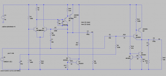
The best way to bridge amps is one of the variations on using the power amp feedback. But a possible useful gadget would be a dual differential buffer where one channel can be cross wired for inversion, using the input jack NC connections. This makes spending $5 on a TL2072 worthwhile. I think +20dBV capability is worthwhile for line level circuits. See attached.
However, I find LV's diode compensation very interesting. As an extension of the idea, see here a VBE+R multiplier load that outperforms a resistor in some ways. The circuit is x10 (+20dB) with no feedback. Note however that loading will compromise the THD because the load will not "compensate" like the active pull-up. A CFP/Sziklai circuit with gain does not have that problem and outperforms wrt THD etc.
Attachments
Last edited:
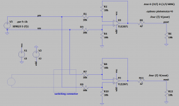
if is it possible can it work with symmetrical voltages (+-12v or-+15 or more)Why not use opamps etc? Well, they may be lower distortion, but they have lots of transistors and I don't think can be as quiet as an elegantly designed two transistor circuit. Hugh forgot that I took his two transistor CFP balanced line driver and made a balanced drive headphone amp out of it. It seems to drive a 49ohm load just fine and with a superb SE Class A harmonic profile. Do we really need 22 transistors and 0.00003%THD, or 2 transistors and 0.03%THD and a beautiful 2nd harmonic profile with descending higher orders?
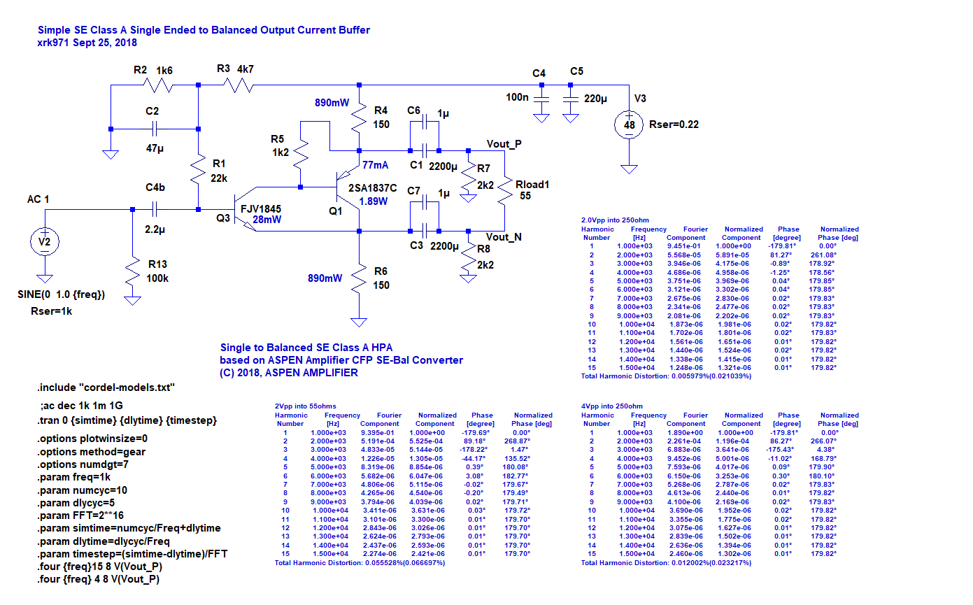
Running at 48v rails and 83mA bias current through a classic 2SA1837 makes for a nice headphone amp. If you used this to drive 600ohm lines, the THD would go way down:
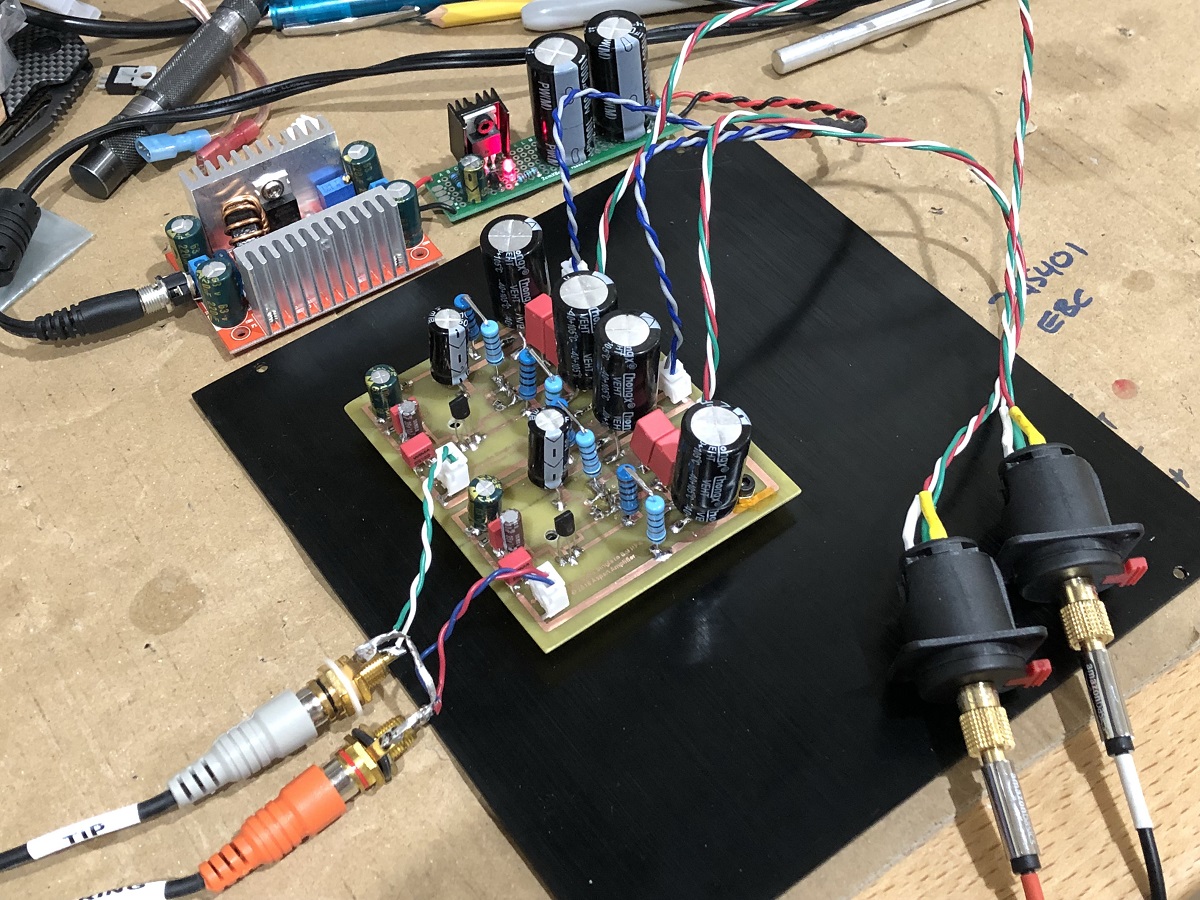
Hand etched PCB:
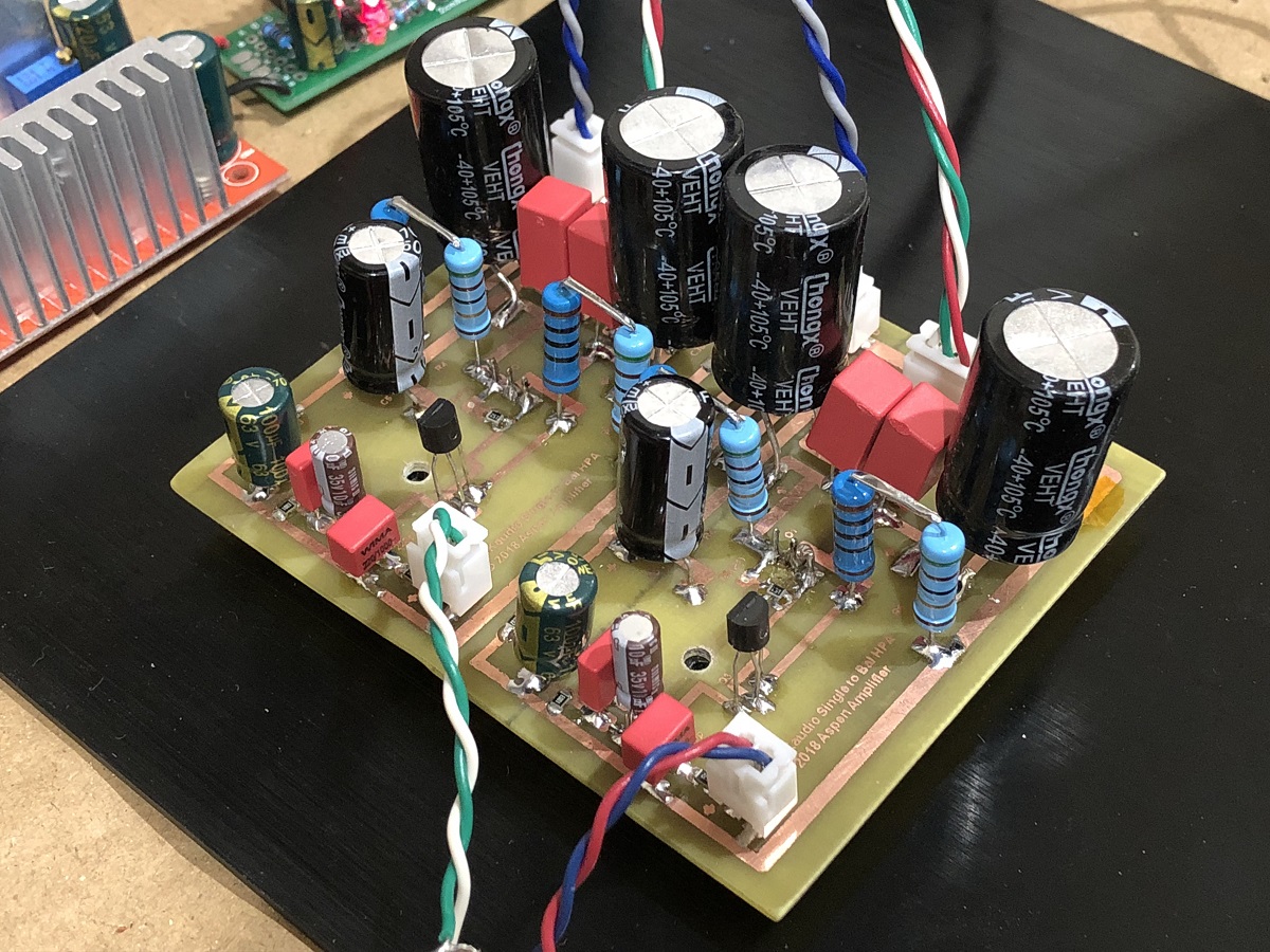
You can see the 2SA1837's underhung mounted here:

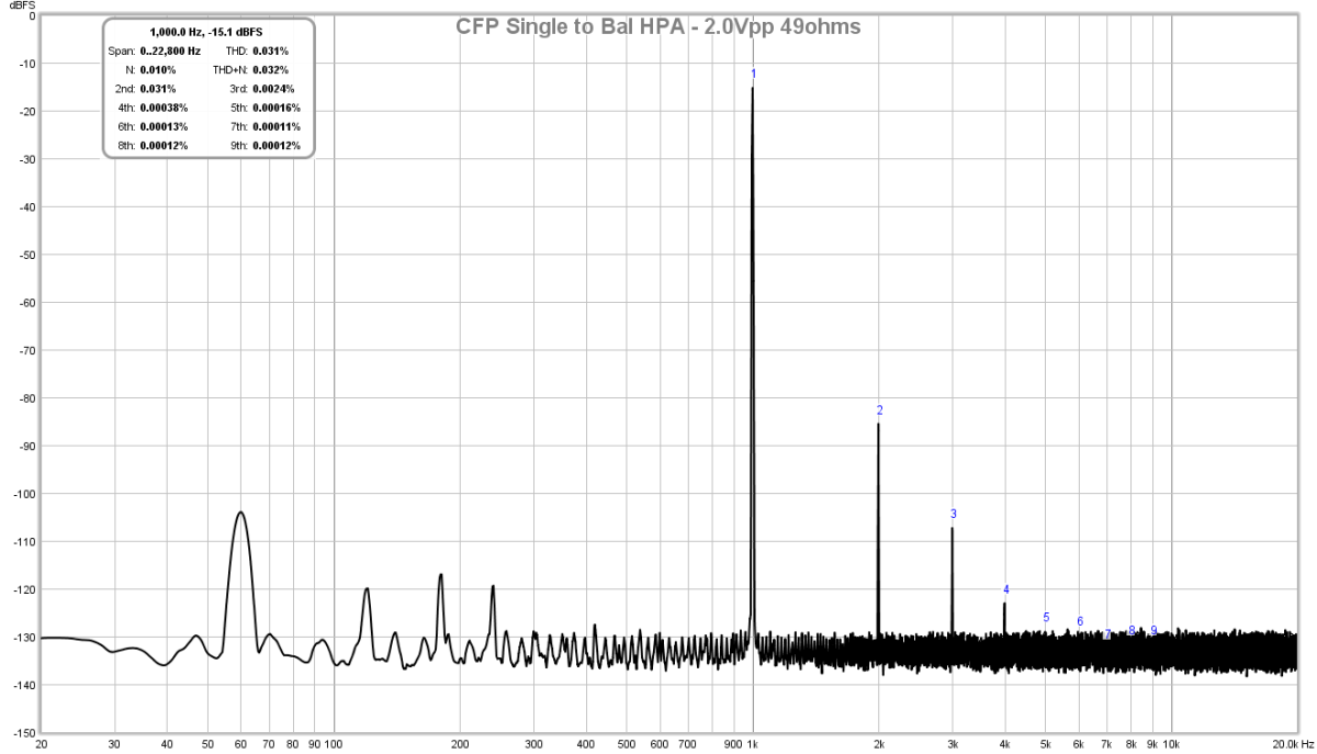
FFT for 2.0Vpp into 49ohm load, THD is 0.03%:
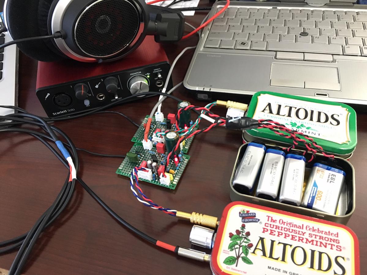
I also made a balanced drive headphone amp using the line-level version of the this circuit to drive a conventional SE Class A headphone amp (two of them, as left and right channels are used as +ve and -ve on same can):
You need to match your parts very closely with that type of circuit for best common mode rejection. It'll work fine though for most applications.Balanced output is easily achieved with a TL072.
It will drive a 180R load easily.
- Home
- Source & Line
- Analog Line Level
- Making balanced output from single end