If they are fast pulse, great.Anybody who has done both, themselves, personally, can see just by observing the shape of the curves, that these measurements are performed with low duty cycle pulses.
I have found considerable variation in temperature dependence and sub-threshold behaviour from different vendors and various structures, so it is not obvious
How can those mosFET models be so far out that the gm result they end up predicting is just not achieveable?
Jay's comment
Jay's comment
may well point to this incorrect gm resulting in bad designs that are not performing as well as the models tell us they should.LTSpice shows very good performance with low bias current (C1381, C1360 and the like) which I strongly believe is not the case in reality.
... but how about BJT models? Because I think I have experienced similar issue with BJT in VAS position. LTSpice shows very good performance with low bias current ... which I strongly believe is not the case in reality.
If it's important to you, get a curve tracer, measure some data on real transistors, and find out. Maybe one of these $229 units will do everything you want. Or maybe the sort of work you want to do, might require higher precision "SMUs" (System Measurement Units; programmable I/O ports with DAC, ADC, V-to-I, etc) than $229 will buy. Then you can step up to a HP4156 or a Keithley 4200. Or you can custom-build a test fixture that measures exactly the data that you want to measure, over the exact range(s) you care about, at the precision that you demand. If it's important to you.
Why not just measure Zout of the regulator with BJT and MOS devices? The issue is, I guess, whether you have to bias up the MOSFET to a level where it behaves linearly.
I am fortunate to have purchased a TEK576 with a decent display. It will cook MOSFETs unless you use the pulsed test fixture (which I don't have.)
I am fortunate to have purchased a TEK576 with a decent display. It will cook MOSFETs unless you use the pulsed test fixture (which I don't have.)
I am a former developer of integrated circuits. In particular manufactured in CMOS technology. I had to develop micro-power generators and stabilizers. I know that most of the models of MOS transistors lie heavily at small (relative to nominal) currents. For digital (switch) schemes is not terrible. Characteristics of MOS transistors Immersed two voltage region on the gate . This is a common area (approximately square law) and subthreshold (exponential law).
The exponential law Id = i0 * exp (Vgs / (n * vt), n> 1 ~ (1.5-5)
==> Gm=Id/(n * vt), vt=26mV.
LTspice in VDMOS model it is possible to use the sub-threshold region.
Hi Sasha
So the Infineon model included in LTspice simply doesn't make use of the LTspice VDMOS model and that's why it is completely wrong in the sub threshold region? I wonder, how hard is it to get a better model for this part for operation in this region?
You'd think that a model 'shipped within' LTspice would at least come with some warnings that it is utterly and completely wrong - like not even in the ballpark - for situations x thru y.
@SGK - that BUK FET looks pretty good (but not as good as the Toshiba here), from eyeballing the datasheet the gm is about 8S @ 1A but notice its measured at 15V, in a regulator you'll probably have lower drop and hence lower gm.
The two BUK just happened to have Spice models shipped with LTspice and when dropped into a model of an AD817-driven Mosfet pass transistor 12V regulator circuit showed extremely good line rejection performance. I'm just wondering if again it is just another case (and this time from a different manufacturer) of untrustworthy LTspice models (at least for this sort of application). I suspect so.
@Mark
The bipolar in your charts is a 'typical profile' or an actual part? I wonder if you have a sample of the BJT used in the Jung/Didden regulator to measure its actual performance...
Last edited:
All bipolar transistors have the same transconductance: gm = Ic / (kT/q) . Here's the relevant part of Chenming Hu's lecture notes @ UC Berkeley.
Of course, an extremely skeptical person might want to disregard Chenming Hu (and Paul Brokaw, and Barrie Gilbert, and Paul Gray, and Richard Jaeger, ... ) and go measure this for himself. I offer my blessings and good wishes for your project, but I won't donate any money or any man-hours to help you execute it.
_
Attachments
The transistor SPICE models do get low current gm, correct. Where they go wrong is largely ignoring Hfe drop and Ft drop
For a VDMOS model in LTSpice, add the ksubthres parameter. IIRC ksubthres is roughly the Vgs per decade Id in the subthreshold region. So if you have a MOSFET with a common subthreshold curve of 250mVgs per decade, start with ksubthres=250mV and adjust it to match the curve.
Just try it, it's not that hard.
Just try it, it's not that hard.
Last edited:
I think it is obvious with MOSFETs, but how about BJT models? Because I think I have experienced similar issue with BJT in VAS position. LTSpice shows very good performance with low bias current (C1381, C1360 and the like) which I strongly believe is not the case in reality.
If you want to find out, here is a PDF from Samuel Groner with many actual detailed measurements of circuits that would be easy to simulate:
http://www.nanovolt.ch/resources/power_amplifiers/pdf/audio_power_amp_design_comments.pdf
Early effect means that at higher current, there will be more harmonics in the base current of a BJT. So depending on the circuit, lower bias can be better.
As anyone might expect, when you introduce a new degree of freedom (a new model parameter), the fitted curve doesn't get any worse. Instead it gets better.
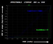
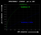
I've plotted the LTSPICE results before (green) and after (blue) adding the new model parameter ksubthres=142m into the VDMOS model of the IPP037N06L3. Compare these plots to Figures 1 and 2 of post #1 in this thread. The curve-fit is improved. As expected. Then the obvious next step is to purchase some more units of the same transistor, hopefully from different manufacturing lots with different date codes, and find the "best" device, the "worst" device, and the "typical" device. Then fit model parameters for all three, allowing simulation with best transistors, worst transistors, and typical transistors.
Armed with a curve tracer and a few samples of a transistor, diyAudio members can perform these tasks themselves. Measure, simulate, tweak model parameters, simulate again, rinse and repeat. Straightforward.
_
Attachments
er... no...Mosfets will never, ever have a higher gm than bipolar, at any current. It's a basic law of physics, which even Scotty cannie change...So said:measured[/I] gm exceeds bipolars. Maybe. Someday. But as far as I can tell, not today.
_
er... no...Mosfets will never, ever have a higher gm than bipolar, at any current. It's a basic law of physics, which even Scotty cannie change...
To elaborate a bit on this, MOSFETs are majority charge carrier devices, meaning they only conduct using one charge carrier, which is electrons in an N-channel type MOSFET, or 'holes' (I like to imagine them like bubbles in water, only the water is electrons) in P-Channel FETs.
BJTs are bipolar devices, which means they use both charge carriers simultaneously, electrons and holes, to conduct current. Hence the 'bipolar' in their name.
Using one type of charge carrier is never going to give better transconductance than using both 🙂.
The main advantage of MOSFETs is that by using only one type of charge carrier, they don't have to wait for that carrier to recombine with a hole to turn off. BJTs, on the other hand, do, and this neutralizing of charge takes time. This makes MOSFETs actual switching speed (in terms of rise time and fall time) much faster, which is why they are so dominant in the modern (and digital) world. When you have switch mode power supplies, digital logic, etc., suddenly the actual speed at which you can turn stuff on and off becomes extremely important, or even the most important property of your switches.
BJTs will always be the transconductance kings, so if that's what you need, BJTs are what you want. They have fallen out of favor largely because of technological context, rather than actually being bested or made obsolete. They aren't used that much because what they're good at is not something we actually do so much these days, while MOSFETs are very well-suited for how we use transistors in the present day.
- Status
- Not open for further replies.
- Home
- Amplifiers
- Solid State
- LTSPICE was wrong: MOSFET transconductance "gm" is NOT higher than bipolar gm