Set the trimmer towards the top, so the Vbe multiplier is set to the minimum voltage (about 0.7V). This will set class C initially.
20mA = 20mV per resistor is a fine starting point. It only needs to be biased into conduction; how far doesn't matter, except that more class A = more power dissipation = more prone to thermal runaway.
2-3 pairs of BD139 would be okay. If using 3 per side, more resistance, perhaps 2.2 ohms per emitter, would be better.
Tim
Would the MJD44H11 be a good transistor for the output in that amp? It doesn't seem to have the gain and speed of the BD139 but not the curviness either, also maybe you'd only need 4 instead of 6. However, it seems the world is out of them until late this year.
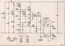
The seperate emitter resistors are *required* to ensure matching of the paralleled transistors. As shown, you have seperate *collector* resistors, which completely defeats the purpose. The common 1 ohm is still required, at least on the bottom side, so the PNP driver transistor knows how much current is flowing on its side.
Complementary (complimentary, notice the "I", means a good comment 🙂 ) would look like this:
http://myweb.msoe.edu/williamstm/Images/Quasi_With_Comp.png
Tim
I really should get a book about amplifier design or something! I was just trying to make it look like the P3A really 😱
Thanks for the complementary output design! So that's ready to go, it can be buuilt as shown there? Perhaps it could also be built with 2 pairs and 1.5-1.8r emitter resistors? I'd have to use 1.2r to test it, hopefully it's stable! The now 22k feedback resistor definately doesn't need the bypass capacitor shown in the original schematic?
Well, I have the complementary version of post #39 running only with 2 pairs of BD139 and 1.2r emitter resistors.
Bias is set to pull around 50ma from the + rail (16v), 12mv accross each 1.2r. No noise or oscillations, just about 2mv RMS of random noise on the output as is expected.
Offset if about 15mv, I will try matching a pair of MPSA18s on the input and see if I can get it any lower.
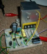
A photo of the breadboard is attached. I have a Hammond heatsink box I'd like to put this in when it's ready, it should provide adequate cooling for any normal listening level. I'd use a bar clamp mounting instead of individual hole mounting as on here.
Bias is set to pull around 50ma from the + rail (16v), 12mv accross each 1.2r. No noise or oscillations, just about 2mv RMS of random noise on the output as is expected.
Offset if about 15mv, I will try matching a pair of MPSA18s on the input and see if I can get it any lower.
A photo of the breadboard is attached. I have a Hammond heatsink box I'd like to put this in when it's ready, it should provide adequate cooling for any normal listening level. I'd use a bar clamp mounting instead of individual hole mounting as on here.
Attachments
remember to match using the same Vbe and the same operational Ic for the devices while holding Vce, Pq, Tc, Tj, at equal values during the testing/matching.
Way overkill.
You will achieve little by comparing hFE using a transistor hFE function integrated into a DMM.
You will achieve little by comparing Ic & hFE if you do not hold Vbe at a known constant voltage.
If you let the device temperature change all your results are wasted.
Not true: when I built the speaker box amps I mentioned earlier in the thread, this is how I matched the small signal transistors for the two LTP stages, and the complimentary final base drivers: pairs with the closest h(fe) and V(be). I got DC offsets measurable in single digits (mV). This transistor matching is a time consuming PITA, but for DC coupled finals, it does pay off for keeping DC out of the speaker voice coils.
Hmm, I matched a pair of MPSA18s and it hasn't helped 😕
Is there another pair which should be matched in this circuit? What does emitter degeneration entail?
Is there another pair which should be matched in this circuit? What does emitter degeneration entail?
I think the 10k resistor at the input should be 22k to match the feedback resistor. This would cause the DC imbalance you're seeing. Try simulating it.
I've left the feedback resistor as 10k in mine, but should the input resistors and feedback be closely matched?
In Sch3mat1c's post #39 schematic, the fbk resistor is 22k. The input to gnd resistor is 10k. These should be the same value, and I think the fbk resistor needs to be 22k (or something around there, 10K would be too low). They don't need to be matched any better than regular 1% or 5% resistors as any offset caused by tolerance differences will be swamped by the LTP devices, even if you match them.
Emitter degeneration usually equalises current in the long tail pair because a resistive element is in series with the BJT´s impedance so it´s a kind of current feedback. It lowers voltage gain but also distortion and extends the open loop frequency response a bit.
The other source of imbalance comes from imbalance in the diff itself. This is controlled primarily by the 4.7k load resistor at the top. Ideally, you want the tail current to be exactly twice 0.7V / 4.7k. You could replace the 4.7k with 2.2k plus a 5k trimmer to null this out. (Remember Ic = Is * exp(Vbe/Vt), where Is is around 10^-12A and Vt is 26mV. If the collector current of one side is e times smaller than the other, the offset will be Vt, or 26mV. e ~= 2.718, so the current imbalance isn't very large at all.)
Offset due to input bias isn't too big a deal, the inverting side transistor should draw about 0.15mA, so its base current will be around 0.7uA. At 10k, the offset voltage is 7.4mV, and same again for 22k, so the total offset is 7.4mV. DC gain is unity, so this amounts to only 7.4mV at the output.
As for the questions I forgot,
1. Quasi because I have a big bag of those 4-0976 things to use up. Dot matrix printers have a lot of these driver transistors, and I took apart several...
2. Ground plane because lots of transistors in parallel can misbehave. A ground plane is the surest way to prevent crosstalk and keep signals in place.
3. The 1 ohm "collector" resistor is there for the benefit of the PNP driver transistor, which makes the whole bottom half look PNP.
4. The MJD44H11 would work fine, but be sure you can heatsink it properly. DPAK transistors are meant to be soldered to the PCB as a sink, which doesn't work very well (even with thermal vias and lots of extra 2oz. board area, you're looking at maybe 10W absolute maximum -- which would be perfectly acceptable for this circuit). The alternate IPAK doesn't seem to be very easy to heatsink, and even with something clamped to it, I don't think more than a few watts is wise. This looks to be intended for switching.
Tim
Offset due to input bias isn't too big a deal, the inverting side transistor should draw about 0.15mA, so its base current will be around 0.7uA. At 10k, the offset voltage is 7.4mV, and same again for 22k, so the total offset is 7.4mV. DC gain is unity, so this amounts to only 7.4mV at the output.
As for the questions I forgot,
why quasi complementary?
Why a ground plane?
Why the extra 1r0 for measuring the output bias?
1. Quasi because I have a big bag of those 4-0976 things to use up. Dot matrix printers have a lot of these driver transistors, and I took apart several...
2. Ground plane because lots of transistors in parallel can misbehave. A ground plane is the surest way to prevent crosstalk and keep signals in place.
3. The 1 ohm "collector" resistor is there for the benefit of the PNP driver transistor, which makes the whole bottom half look PNP.
4. The MJD44H11 would work fine, but be sure you can heatsink it properly. DPAK transistors are meant to be soldered to the PCB as a sink, which doesn't work very well (even with thermal vias and lots of extra 2oz. board area, you're looking at maybe 10W absolute maximum -- which would be perfectly acceptable for this circuit). The alternate IPAK doesn't seem to be very easy to heatsink, and even with something clamped to it, I don't think more than a few watts is wise. This looks to be intended for switching.
Tim
Yuck, capacitor coupled (better unplug your speakers before turning it on/off!), no differential! 1979, I thought those things went away in the 60s. 😛
Guess you can't argue with the simplicity. Having all of five transistors, it would be very cheap to make. Hence why it's often seen in cheap consumer electronics of the period. 🙂
Tim
Guess you can't argue with the simplicity. Having all of five transistors, it would be very cheap to make. Hence why it's often seen in cheap consumer electronics of the period. 🙂
Tim
Interesting design, but capacitive coupling is to be avoided, especially seeing as I have the +/-18V supply already!
I will be building Sch3mat1c's design, but it will be quite a while. I will be building a stereo amp with 2 pairs of outputs on each channel onto stripboard 🙂eek🙂 and into a small Hammond heatsink box. It will include a volume control, headphone amplifier and 'digital' on-off switching 🙂
I will be building Sch3mat1c's design, but it will be quite a while. I will be building a stereo amp with 2 pairs of outputs on each channel onto stripboard 🙂eek🙂 and into a small Hammond heatsink box. It will include a volume control, headphone amplifier and 'digital' on-off switching 🙂
A dissapointing update...
Sorry for delay in update, I was on vacation.
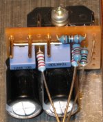
So, I built Sch3mat1c's design on stripboard:
and it seemed promising. I powered it up (it's one half of a would of been stereo board) and got 8mv offset at output, minimal noise showing on scope. I then connected a test speaker and got buzzing when I touched the input, so that was promising too. I then tried to set the bias... 😱
I've done it on many amplifiers before without issue. I attached a block of aluminium to the outputs as a temporary heatsink and advanced the multiturn pot with a multimeter connected accross one of the 1.5R resistors. I kept turning it, it's a 25 turn pot and I knew it had to go quite a way, still 0mv showing on the meter. I think that a crocodile clip lead I was using to connect the meter to the resistor was at fault, they have been intermittent with other applications too; it's not a good show when you can't trust your test equipment! So, I never got any reading but I caught a slight 'hot' smell and touching some parts confirmed this, I can only assume the wiring was correct but the bias was inadvertently set way too high.
I now get the same readings for any setting of the bias, different values accross each 1.5R output resistor. Something like 54mv, 10V 🙂eek🙂, 6mv and 0.1mv! I think the words 'beyond repair' spring to mind
I'm afraid I'll probably have to resort to plan B, using LM1875 chip-amps! Fortunately, I can use a vast majority of the parts I bought for this and I have a pair of LM1875s already. I will be careful with them . I'm thinking either point-to-point or stripboard again, no PCB design fits my requirements and I've never had any luck making my own. They will be mounted with a bar clamp, as the discrete design would have been.
Sorry for delay in update, I was on vacation.
So, I built Sch3mat1c's design on stripboard:
An externally hosted image should be here but it was not working when we last tested it.
and it seemed promising. I powered it up (it's one half of a would of been stereo board) and got 8mv offset at output, minimal noise showing on scope. I then connected a test speaker and got buzzing when I touched the input, so that was promising too. I then tried to set the bias... 😱
I've done it on many amplifiers before without issue. I attached a block of aluminium to the outputs as a temporary heatsink and advanced the multiturn pot with a multimeter connected accross one of the 1.5R resistors. I kept turning it, it's a 25 turn pot and I knew it had to go quite a way, still 0mv showing on the meter. I think that a crocodile clip lead I was using to connect the meter to the resistor was at fault, they have been intermittent with other applications too; it's not a good show when you can't trust your test equipment! So, I never got any reading but I caught a slight 'hot' smell and touching some parts confirmed this, I can only assume the wiring was correct but the bias was inadvertently set way too high.
I now get the same readings for any setting of the bias, different values accross each 1.5R output resistor. Something like 54mv, 10V 🙂eek🙂, 6mv and 0.1mv! I think the words 'beyond repair' spring to mind
I'm afraid I'll probably have to resort to plan B, using LM1875 chip-amps! Fortunately, I can use a vast majority of the parts I bought for this and I have a pair of LM1875s already. I will be careful with them
. I'm thinking either point-to-point or stripboard again, no PCB design fits my requirements and I've never had any luck making my own. They will be mounted with a bar clamp, as the discrete design would have been.
Last edited:
Hi,
I've started a build thread for the chipamp. It's a very compact design and calls for a board with the chips located to mount over the 'rails' inside the heatsink box and the chips must be mounted under the board for this too. The stripboard appears to be working and I doubt I could get it more compact on a PCB. A PCB may offer better performance, at higher power especially, but this won't be used at any power much over 1W.
http://www.diyaudio.com/forums/chip-amps/168553-lm1875-miniature-desktop-amplifier-build.html
🙂
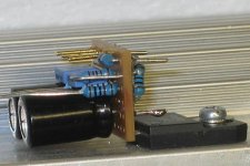
Here's my compact LM3875. 😀
Attachments
Last edited:

- Status
- Not open for further replies.
- Home
- Amplifiers
- Solid State
- Low power discrete designs?