What's the point in quoting silly power numbers?Segran said:When re-doing the measurement I got 70 Vp-p across a 7R resistive load and 80 V p-p across my 8 ohm speakers (sine wave 1kHz). That's 10 A p-p, 800 W p-p! Not bad for TIP35/36 without drivers...
80Vpp=40Vp=28.3Vac. Those are equivalent to 100W into 8ohms.
Yes that's pretty good for TIPs.
But, you must consider reactive loading.
The least you can expect to make an effective 8ohm capable amplifier is to be able to drive a 4r0 (resistive) load to full power, i.e. ~180W into 4ohm.
However, most 8ohm speakers will stress the output stage even more than that 4r0 test. You really need to check the temperature de-rated SOAR curves for reactive loads before making the decision that this TIP based amp can run on those supply voltages.
Yes, those are silly numbers, that's what some companies (SONY, Pioneer etc) use in their advertising. Or at least they used to do in the 80's.
I know that the TIP35/36´s are operating outside SOA, but they are obviously much more "robust" than the TIP142/147's suggested by you. I'm waiting for 2SA1943/2SC5200 to arrive in the mail. They should be on the safe side, don't you think?
Still, it is a "silly" project by all expert opinions, I should have used MOSFET's instead, or included drivers.
I have learned quite a lot during this project, from you and megajocke in particular Thats more valuable to me than the specific data on the amp. I'ts been more than 30 years since i made any analog design so may previous knowledge is perhaps outdated and absolutely rusty.
In my next project I hope to gain your approval as well!🙂
megajocke said:
Look att coffin's amp, the whole amp is built that way! 😎
OOPS
not mine!

Segran said:I know that the TIP35/36´s are operating outside SOA, but they are obviously much more "robust" than the TIP142/147's suggested by you. I'm waiting for 2SA1943/2SC5200 to arrive in the mail. They should be on the safe side, don't you think?
...
In my next project I hope to gain your approval as well!🙂
Why don't you run some simulations to see whether your design is safe or not? LTspice is a very good simulator!
Attachments
I would, if I could. Can't find models for those transistors, and I'm not familiar with Spice modelling.
I have tried but gave up.
I have tried but gave up.
Segran said:I would, if I could. Can't find models for those transistors, and ...
For SOA, you don't need to have the modules. Just like the example I quote you just need to see the curve (Ic vs Vce) of your circuit. I used small signal transistors to get the data. The simulation circuit won't blow up.
Sorry, I ment 2SA1943/2SC5200! Toshiba don't seem to give any Spice support. I will give it another go thanks to the help you are giving me. Have never used Spice before and I find the UI a bit far from what I am used to......
Segran said:Sorry, I ment 2SA1943/2SC5200! Toshiba don't seem to give any Spice support. I will give it another go thanks to the help you are giving me. Have never used Spice before and I find the UI a bit far from what I am used to......
You can find these device models on the Fairchild website.
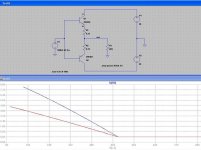
Thanks, I have got those models as well now, will try them tomorrow. I can't get the step function for RL to work, but here is the result for TIP35C/TIP36C 4hm load. I'm not worried that they will fry anytime soon after seeing this..
Thanks, I have got those models as well now, will try them tomorrow. I can't get the step function for RL to work, but here is the result for TIP35C/TIP36C 4hm load. I'm not worried that they will fry anytime soon after seeing the plot. Can't share, I don't know what resolution/pixels to use.
Thanks, I have got those models as well now, will try them tomorrow. I can't get the step function for RL to work, but here is the result for TIP35C/TIP36C 4hm load. I'm not worried that they will fry anytime soon after seeing this..
New attempt - with driver stage
Here's my latest attempt with LME49810/49830. While I'm working on the layout it would be nice to get your comments! It turned out to be very helpful the last time.
I probably got a bit carried away with decoupling cap's, adice and suggestions on that topic as well as anything is higly appreciated.
Here's my latest attempt with LME49810/49830. While I'm working on the layout it would be nice to get your comments! It turned out to be very helpful the last time.
I probably got a bit carried away with decoupling cap's, adice and suggestions on that topic as well as anything is higly appreciated.
Attachments
R4 should probably be 0 ohms, but there's no harm including it in the PCB so you can use one if the bias is overcompensted. It's also best if P1 and R14 switch places (new values needed of course) so that an open or intermittent wiper will cause underbias instead of a burned output stage.
C3, C27 - best is if these are not needed, but include them in the board so you can add them if the output stage is unstable.
What's up with the circuit around U1B? You have 0.33µF loading the input signal. Why the convoluted feedback and input signal stuff? Why a DC servo AND C23? The goal of DC servo is usually to eliminate the large capacitor in the feedback. The DC servo doesn't look right either.
If you plan to drive 4 ohm loads you should use 2 pairs of output transistors, for 8 ohm loads 1 pair should work fine.
The overall gain is very high
stage 1 2times, +6dB.
stage 2 37times, +31.4dB.
combined gain +37.4dB.
I don't understand all the extra cap coupling around various parts of the circuit.
I pair of To264 on +-55Vdc is asking a lot, even into 8ohm loading.
stage 1 2times, +6dB.
stage 2 37times, +31.4dB.
combined gain +37.4dB.
I don't understand all the extra cap coupling around various parts of the circuit.
I pair of To264 on +-55Vdc is asking a lot, even into 8ohm loading.
"I pair of To264 on +-55Vdc is asking a lot, even into 8ohm loading."
That or one pair of the just smaller TO-3P:s is what you will find inside almost any commercial amp. 4-ohm capable amps hopefully have two. I assume 55V is the unloaded voltage.
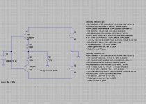
The attached image shows a simulation for +-50V ideal non-sagging supplies and a 6 + 8j ohms load (about 60 degrees phase angle) just before clipping which is worst case for reactive loads >= 45 degrees. 45 degrees will give a little lower peak powers and temperatures. Frequency is 30Hz, chosen low for worst stress on transistors.
The simulation is done with the FJL4x15 thermal model, .4 K/W case-heatsink, 75 degree C heatsink, thermal capacity of package was chosen as 1K/J (it should be higher in reality but this only matters for >100ms times).
It can be seen that thermally this is not a problem, second breakdown shouldn't be a big problem either at this low voltage supply - it can take 350W for 100ms at this voltage single pulse or 600W single pulse for 10ms. The pulses are 10ms but not square but half-sine-ish, making the calculated 200W pulses equal to somewhat lower square-pulses. If it can take 350W for 100ms single pulse without second breakdown it should be able to take 120W or so for 10ms repetitive without any problems at all as long as temperature is kept within reason.
Average dissipation is 40W transistor.
That or one pair of the just smaller TO-3P:s is what you will find inside almost any commercial amp. 4-ohm capable amps hopefully have two. I assume 55V is the unloaded voltage.
The attached image shows a simulation for +-50V ideal non-sagging supplies and a 6 + 8j ohms load (about 60 degrees phase angle) just before clipping which is worst case for reactive loads >= 45 degrees. 45 degrees will give a little lower peak powers and temperatures. Frequency is 30Hz, chosen low for worst stress on transistors.
The simulation is done with the FJL4x15 thermal model, .4 K/W case-heatsink, 75 degree C heatsink, thermal capacity of package was chosen as 1K/J (it should be higher in reality but this only matters for >100ms times).
It can be seen that thermally this is not a problem, second breakdown shouldn't be a big problem either at this low voltage supply - it can take 350W for 100ms at this voltage single pulse or 600W single pulse for 10ms. The pulses are 10ms but not square but half-sine-ish, making the calculated 200W pulses equal to somewhat lower square-pulses. If it can take 350W for 100ms single pulse without second breakdown it should be able to take 120W or so for 10ms repetitive without any problems at all as long as temperature is kept within reason.
Average dissipation is 40W transistor.
Attachments
"R4 should probably be 0 ohms" - CORRECT! I used 10R in the previous version, but can just as easy be a 0R jumper. Anyone know why almost all published designs use 1k2 before a trimmer of 200R-2k and then a approx 360R resistor? Those values doesn't seem to work... 
"C3, C27 - best is if these are not needed" - CORRECT again, they are not supposed to be mounted on the BJT version, only on the MOSFET. But now I can't find the article describing this, it had to do with MOSFETS being too slow/too fast when shutting off.... 😕 So they are gone, but I'll keep them in for the layout.
"What's up with the circuit around U1B? Why the convoluted feedback and input signal stuff? Why a DC servo AND C23?" Well, as in my previous TIP based amp, I stole this from P-A Sjöströms Gainclone amp. It seems to work fine there, as it also do in the TIP amp. But P-A's design holds a lot of options and I may have stolen too much. Your are right in that the input stage creates a heavy load on the input signal... Will try to loose at least C7, possibly also C17/C21 in ,y Gainclone first to see what happens. Have checked the schematic of the DC-servo and it's correct. It works fine both in my Gainclone and the TIP amp, reducing DC level from 25-30mV to 2-3 mV. But I am thinking about chucking both the input stage and the servo in the bin. Seems to be a negative bang-for-the buck analysis...
The plan is (was) to use 8ohm speakers since that is what I have. But then again, who knows what I will use tomorrow... When working on the layout I have been thinking about separating the output stage from the driver all togehter, as this would give me more flexibility for the future. Any advice on how long wires I can have between driver stage/output stage? I'm thinking in the range 20-30mm upto 100-150mm to be able to spread the transistor eavenly over the heatsink surface.
The heatsink is 40 mm thick x80 mm high x 300 mm long, one for each channel. They should give Rt=0,55 dgr C/W. That should be fine for 2 transistors/8ohm but probably to small for 4 transistors/4 ohm. On the other hand, it is highly unlikey that I will ever use more than 40-50W in avg (I'm not deaf yet..) and I have already the heatsinks/box.
I don't have the transformer yet so I still can play with the rail voltage. The tranny I (had) decided for is a 2x40V 400VA or 500 VA, but I guess I could go down to 2x35V, same VA rating. I have a 2x24V 400VA, but 33V rails compared to 48 or 55V seem to be an overkill in the wrong direction. And yes, I have calculated with approx. 1V drop across the rectifier diodes, hence the 1 V lower figures I use compared to straight x1,414...
What is your best recommendation on this? 😕
"The overall gain is very high" - Yes, I have used arbitrary values in the NFB without doing any maths... Any suggestion for the "ideal" gains for each stage? 😕
"CORRECT! I used 10R in the previous version, but can just as easy be a 0R jumper. Anyone know why almost all published designs use 1k2 before a trimmer of 200R-2k and then a approx 360R resistor? Those values doesn't seem to work..."
I believe you might have read the schematics wrong, there is almost never a resistor outside the E-C of the transistor. Usually there are two resistors and one pot in the divider to give the pot reduced range so you can set it with more accuracy.
I understand then why the input circuit looks like that. You are supposed to be able to choose between inverting/non-inverting buffer, inverting/non-inverting main amp, DC-servo or coupling cap. The DC servo can be returned to either positive or negative input and can thus be made an inverting integrator or a buffer with RC filters.
Right now you have a mix of all of them, circuits are working against themselves.
Too much copy-paste... Yesterday I cleaned up the input stage and the DC-servo circuit to only reflect NI/NI with DC-servo. P-A Sjöström doesn't use clamping diodes on the DC-servo input of the NI/NI version, but when testing on one of my GainClones it went hay-wire without them.
DC-level on the output is now dead zero compared to 5-6 mV before. And it sounds much better....
I have taken your advice for the VBE circuit, values are to be confirmed when testing.
Any advice on the length of wires between driver board and second output stage? I have made provisions on the PCB to connect a second driver stage.
Have also included +/-15 V regulators and pre-regulators to feed the low voltage regulators straight from the power amp rails.
Schematics with the latest, probably not last, updates comes here:
Attachments
- Home
- Amplifiers
- Chip Amps
- LME49810 - a new cousin for LM4702