hi guys,
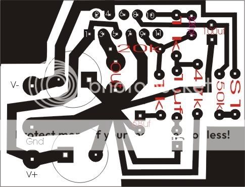
please check my one sided LM3886 pcb layout, thanks
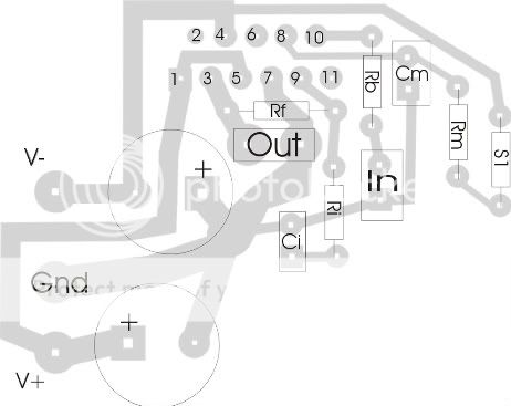
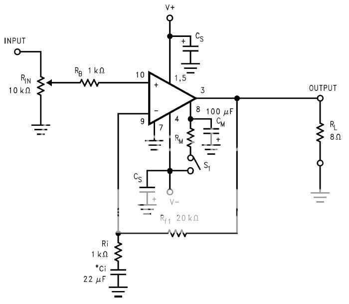
here is the schematic
note: input potentiometer is omitted on the pcb
please check my one sided LM3886 pcb layout, thanks
here is the schematic
note: input potentiometer is omitted on the pcb
Hi,
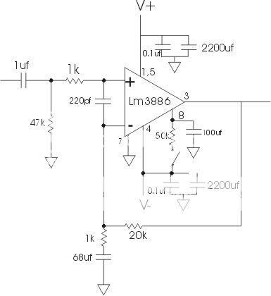
you pulled the schematic from the National datasheet.
But, you forgot to read the rest of the datasheet.
As a result you have omitted many components that are recommended by National.
Start again.
you pulled the schematic from the National datasheet.
But, you forgot to read the rest of the datasheet.
As a result you have omitted many components that are recommended by National.
Start again.
Big, unconnected copper areas are an absolute no, no. Either connect them to ground or use that space to make some fixing holes.
Leave some room between the copper and the PCB's border. Remember that a PCB will be produced on a bigger piece of board, which will later be cut to size. Copper right at the cutting edge is likely to be damaged during that process.
Try to keep straight paths at right angles, and make turns at 2x45°. Looks also count. And put yourself into the place of an electron. You are travelling through the copper at nearly the speed of light, and then suddenly there is a 90° turn in front of you. Boy, will you hit your head.
click me
The resistor between signal and power ground can help you with hum issues. You may not need it, but your PCB should be prepared to refit it.
Just a friendly reminder, and I quote from wikipedia, because my physics textbooks are too far away from my desk:
It is only when considering group velocity that electric current moves rapidly (think of toppling dominoes).
For High Frequency work, those layout guidelines matter. For audio, not so much - just look at the sample PCB's in the datasheets for some of the National chipamps. You're quoting from a guide to switchmode power supplies, which are indeed high frequency devices.
All that said, I hate it when components on a PCB don't sit straight, and I'd never make one up from random angles myself, but that's for purely aesthetic reasons. If it looks good, it'll work well, everything else being correct.
http://en.wikipedia.org/wiki/Electric_current#The_drift_speed_of_electric_charges
Electric currents in solids typically flow very slowly. For example, in a copper wire of cross-section 0.5 mm², carrying a current of 5 A, the drift velocity of the electrons is of the order of a millimetre per second
It is only when considering group velocity that electric current moves rapidly (think of toppling dominoes).
For High Frequency work, those layout guidelines matter. For audio, not so much - just look at the sample PCB's in the datasheets for some of the National chipamps. You're quoting from a guide to switchmode power supplies, which are indeed high frequency devices.
All that said, I hate it when components on a PCB don't sit straight, and I'd never make one up from random angles myself, but that's for purely aesthetic reasons. If it looks good, it'll work well, everything else being correct.
Pin 7 to power ground. The currents from this pin are not clean.
0u1F decoupling? On the back adjacent to the chips power pins?
Use the space just to the left of pin 2 to insert these small decoupling caps. Tie the junction of these caps to the power ground using a short link.
Zobel from output to power ground?
Remove the trace from power ground to signal ground. Insert a pair of holes for a link/resistor to tie these together.
There are sufficient pins to support this chip to the PCB. Break off the three unused pins and use the space freed up to ease your routing.
Q.)
Where should pin 8 go? Is it clean enough to tie into the signal ground or should it go to the power ground?
Thanks for the reminder. I had not forgotten my lessons on that, so no need for text books. Using the same hydraulic model that explains, why individual electrons travel slow, while currents seem to travel near the speed of light will lead to the same result. Avoid right angles.TheSeekerr said:Just a friendly reminder...
The imagination of the electrons traveling so fast and banging their heads is easier to explain, easier to remember, and not too far from the truth. So, they bang their heads more slowly? Bet it still hurts.
Yes, they do. The difference is that in audio you can get by with a bad design, because it only affects the quality, and most of the time below audible perception, while in HF it can seriously affect the function.TheSeekerr said:For High Frequency work, those layout guidelines matter. For audio, not so much
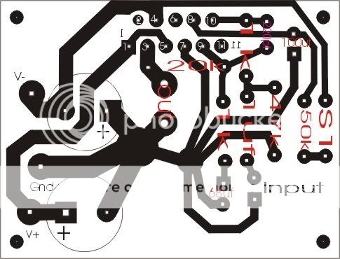
ryan750 said:hi,
i this ok??
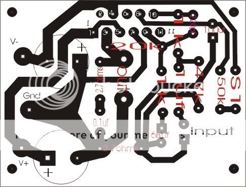
This one is good, you are getting closer now. I feel the power supply Cap in v- and gnd can be rotated by 90 deg to have more thickness for v+ track. and +v, -v and gnd can be aligned vertically.
do as Kuldeep says.
Remove pin 2 and sort that supply rail bottle neck.
Push both smoothing caps up and that allows your PCB to be smaller.
I too think that pin8 should go to power ground, but I'm not sure. anyone else????
you could break the connection to signal ground and place 3 pin pads @ 0.1inch centres to allow experimentation. There's space for that.
@ kuldeep
i've done what you've suggested. tnx
🙂 🙂 🙂 🙂
@ andrew
tnx for posting
btw i don't feel like snipping the pin 2 so i've just widen the track
i've connected pin8 at the power ground
what about the pads??? where im gonna put that?
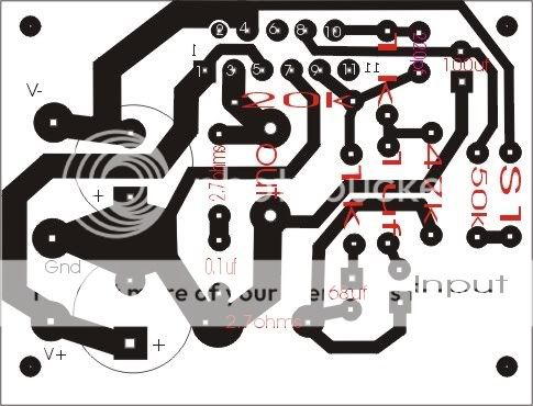
i've updated the layout
i've done what you've suggested. tnx
🙂 🙂 🙂 🙂
@ andrew
tnx for posting
btw i don't feel like snipping the pin 2 so i've just widen the track
i've connected pin8 at the power ground
what about the pads??? where im gonna put that?
i've updated the layout
go for a prototype
make an actual pcb of the latest layout, sometimes you get ideas after working on the actual hardware.
as andrew said, i also feel pin 2 can be simply removed from the IC, widen the -ve coz anyway pin 2 is a n/c pin, it has no purpose. and pin 8 connection is correct.
make an actual pcb of the latest layout, sometimes you get ideas after working on the actual hardware.
as andrew said, i also feel pin 2 can be simply removed from the IC, widen the -ve coz anyway pin 2 is a n/c pin, it has no purpose. and pin 8 connection is correct.
If you don't fell like snipping the n/c pins, you can integrate them into your traces. E. g. pin 2 can be connected to V- without drawbacks. That way the V- trace can become wider. All n/c pins are truly not connected inside the IC, so they can be connected anywhere just as well as be left disconnected.
hi friends please any one send me the lm3886 amplifier circuit with pcb layout to shravanth.reddy@yahoo.com
- Status
- Not open for further replies.
- Home
- Amplifiers
- Chip Amps
- lm3886 single sided pcb