it's ok layout , simple..thanks for the reply guys,
here is the updated pcb layout, anything wrong??
Hello my dear ... I found this nasty PCB design and came up with my own EVEN WORSE! and horrible star grounding solution that no ordinary noob would use...
uploading pictures
What would i change , there will be stereo version with just 2 of them wired to 250VA toroidal transformer wich has 4 outputs quad 24V
And for power supply, alot small 3300uF 50V non ebay electrolytic smokers..
An externally hosted image should be here but it was not working when we last tested it.
uploading pictures
What would i change , there will be stereo version with just 2 of them wired to 250VA toroidal transformer wich has 4 outputs quad 24V
And for power supply, alot small 3300uF 50V non ebay electrolytic smokers..
Last edited:
In both posts 21 & 22, I can see that the Power Zero Volts is not associated with the Power Rails.
This creates an enormous loop area that will emit radiation.
Have a think about where the current that flows out on the +ve supply rail and which leads and traces does that current follow to get back to the start from whence it came.
REMEMBER all electricity flows in circuits. Circuits is a sort of "circular route" every current must come back to it's source.
I may be naive but would anyone ask to have the schematic and layout sent to them when both are attached to the thread?
I really didnt want to make new thread about the same thing...
image hosting site no sign up
I think this could work out, i still dont understund :/
An externally hosted image should be here but it was not working when we last tested it.
image hosting site no sign up
I think this could work out, i still dont understund :/
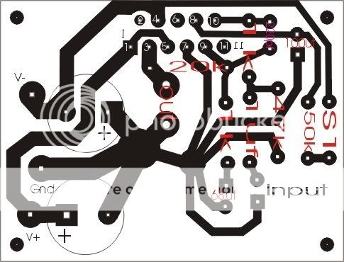
Why the big LOOP AREA in the power input connections to the big caps?
I cannot see any HF decoupling at the chip power pins.
The signal input looks good with lowish LOOP AREAs. Look at the gap between the traces going to Pins 9 &1 0 !!!! You could make the loops even smaller, especially since you have a 2sided PCB. Pin11 pad could be removed completely and just use the remaining 10 pins to mount the chip. You have already used the n/c Pin2 properly.
It might be fine for now but the power input side seems fishy to me, arent my power rails a bit too long?
print screen windows 7
An externally hosted image should be here but it was not working when we last tested it.
print screen windows 7
The power rails must be close together and caps can be smaller wich i dont like... still they will help.
What about filled plane ground?
picture hosting
But thank you AndrewT
Seems like you are like somekind of "Grandmaster" on this forum?
I just wanted to design a very fine single sided board but it seems "impossible" some are saying "JUST MAKE THE POWER RAILS AS WIDE AS YOU CAN AND GND CAN BE THIN!"
But some current must get trought and i should keep them both balanced just to the point when they work out best...
What about filled plane ground?
An externally hosted image should be here but it was not working when we last tested it.
picture hosting
But thank you AndrewT
Seems like you are like somekind of "Grandmaster" on this forum?
I just wanted to design a very fine single sided board but it seems "impossible" some are saying "JUST MAKE THE POWER RAILS AS WIDE AS YOU CAN AND GND CAN BE THIN!"
But some current must get trought and i should keep them both balanced just to the point when they work out best...
Last edited:
Use two small caps instead of one, from each rail to gnd, and close as possible to power pins. There is already enough space.
Move large caps close as possible to power pins and add another in parallel, for each rail. Even better would be to also add a smaller one closer to pins, say 470 or 330 uF, since larger ones can't get close enough.
Eliminate the gap between the signal traces as much as possible.
No need for ground between power rails, necessarily. But maybe center the gnd input for better symmetry.
Last edited:
The best ive been able to do is this one:
picture share
I love big caps or many small caps...
An externally hosted image should be here but it was not working when we last tested it.
picture share
I love big caps or many small caps...
The HF decoupling is at the wrong end of the supply rail traces.
The HF decoupling should be at, or on, the chipamp power pins.
The HF decoupling should be at, or on, the chipamp power pins.
AndrewT is correct. Maybe I wasn't clear about which pins.
Also, the input traces still have a larger-than-necessary area between them, which makes them a better antenna for both hum and RF. You will also want to tightly twist together the input wires from the jack to this board, as well as all of the wire pairs that connect to the transformer(s).
I would also want to be prepared to have the input signal ground not be connected to the power and speaker ground, and instead have its own wire back to the psu output ground. You should have pads for a series resistor or jumper or nothing, in the trace that connects the input ground to the main ground.
The currents in the main ground's wire to the psu will induce time-varying voltages across the inductance and resistance of the wire itself, which will effectively be summed with the input signal.
Last edited:
The HF caps will be soldered directly to legs.
Thanks AndrewT and gotee.
Seems like a plan, so i remove the rail to the input ground and add pad for fire that is connected to power supply ground.
I will twist the cables and keep them short, input signal cables will be fully shielded (Foil shielded cable)
Now the power supply?
software screenshot
Thanks AndrewT and gotee.
Seems like a plan, so i remove the rail to the input ground and add pad for fire that is connected to power supply ground.
I will twist the cables and keep them short, input signal cables will be fully shielded (Foil shielded cable)
Now the power supply?
An externally hosted image should be here but it was not working when we last tested it.
software screenshot
The upper HF decoupling (-ve) route is quite short.
Have you tried to draw the route that the current must take through the lower of the HF decoupling (+ve) capacitors?
It seems you just don't understand what inductance is, or why it is not good for HF current transients, or why it can be big and how to help make it small.
Similarly look at the input current routes.
Remember than the input is a two wire connection. Signal Hot and Signal Return.
Draw out the whole route that the input current must follow. You will then see the big loops in your proposal.
Last edited:
Have a look at this elektor electronics magazine design
here is the Pcb i made
http://www.ebay.in/itm/230976792076?ssPageName=STRK:MESELX:IT&_trksid=p3984.m1555.l2649
Attachments
The two small caps cannot do their job if they are connected more than a couple of mm from the chip's power pins.
Don't think of the caps as filters. Think of them as current sources for fast transient signals. Then you can see that inductance between caps and power pins degrades their peak performance. Then realize that more conductor length equals more inductance.
Also remember that all loops should be as small as possible. Then also think of the loops of current from caps to power pins to ground and back to caps. Make those loops as small as possible. And make smallest caps have smallest loops.
Last edited:
Good work🙂
I have bought 16 of them so far from Rajudp.
Good work, Rajudp. Just a few "fine points":
On the PCB, I would like to see the input ground trace/plane stay closer to the input signal trace, and it should stay next to the signal trace all the way to the input pin, to minimize the "enclosed loop area" that is enclosed by the signal and signal ground conductors, which forms a magnetic antenna for hum (and also for RF). So the ground copper that connects to the "ground" end of R2 should also be extended by being poured under R1, and C1, and under R2 and C2, and all the way until it is near the input pin.
Also, if you don't use an extremely-large (very low impedance) conductor to connect the board ground to the star ground and power supply caps' ground, then there will be significant unwanted voltages induced across the ground conductor itself (across its parasitic inductance, and also resistance), by the speaker return current and the decoupling caps' ground currents, which will then be arithmetically summed with the input signal (!), which is not a good thing.
Star grounding should be used, instead. i.e. The input signal's ground reference point, i.e. the ground end of R2, should have its own completely-separate wire that goes all the way back to the star ground or the power supply output ground.
And probably the speaker ground should also go directly from the speaker terminal to the star ground or the power supply ground, or, it should have a separate ground wire from this board to the star ground or PSU ground (but staying close to the other PSU wires).
And, of course, C7 and C8 are useless, in their current positions. They MUST be located directly AT the power pins of the chip amp.
Last edited:
- Status
- Not open for further replies.
- Home
- Amplifiers
- Chip Amps
- lm3886 single sided pcb