That's probably OK.So, a bit of progress update.
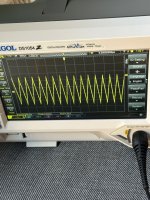
I built a DAC today based on the PCM1681. I don't have any speakers hooked up currently, but I watched the waveform on the output of it, and when I use the Beep Tone on the STA310, which the documentation says is a triangle wave, it shows up just fine as a triangle wav on the scope. So far so good.
You need to turn on the OVER feature of the DAC to push the ripple farther in frequency. Thereafter, a 2nd LPF around 25kHz would fix it. You can see my DTS 1536 waveforms (full scale) at the link below, the shape is very much sinusoidal.When I do dolby digital though, I can see the waveforms, and they follow along with what the TV shows, but the signals seem to have more noise than signal. I'm not sure if this is clock jitter or where it's coming from, but it's a very noisy representation of the audio waveform. I know it needs to go through a low pass filter next, but it seems pretty messy at this stage, and I'm not sure a LPF will fix it.
https://www.diyaudio.com/community/...references-opinions-ideas.381423/post-7198960
Thanks. I’m still a bit stumped what’s going on. It doesn’t help that the documentation conflicts in certain areas. I’ll wait until I get the new DAC that I can hook up and connect headphones too. My gut says there’s an issue with the clocks and/or the format.
For the data format, STA 310 has a right padding bit. I’m confused what it does as the description in the manual and the implementation guide conflict. Ie the docs say it does one thing, but in the example they do the opposite and the comment says the same thing.
1) triangle wave looks fine at the DAC output, but only if I apply attenuation in sta310 via registers. If I don’t, the tips of the triangle seem to fold over. I don’t think it’s clipping as they aren’t cut off, it’s like the DAC values start decreasing at the top of the triangle instead of increasing. Makes me thing it’s formatting at the stream level.
2) but I’ve tried ever combination between the formats and I can’t seem to make it jive
3) Dolby digital output is hardly noticiable on the scope and noisy. The noise starts as soon as I enable the clocks via the mute and play register. It’s not even decoding yet and the DAC output is noisy. It’s clean right up until clocks are engaged. The only way I can think that would happen is if the clocks are noisy and the DAC is latching onto random 1s when they should be zero.
Not sure. I’ll play with that DAC tomorrow but then maybe stew on it a week.
Attachments
If I remember correctly, you can't skip the post-processing commands even if you don't use any volume, bass redirection, delay or prologic. Also, the autodetect interrupt does not work in the idle mode, it works only if some decoding algorithm is loaded. That's why I load the PCM decoder immediately after startup.
You can get some audio out with just a simple RC filter for the time being. There're only two formats, I2S and Sony to select from, one of them will fit your DAC's input format (LJ).
You can get some audio out with just a simple RC filter for the time being. There're only two formats, I2S and Sony to select from, one of them will fit your DAC's input format (LJ).
Last edited:
If I remember correctly, you can't skip the post-processing commands even if you don't use any volume, bass redirection, delay or prologic. Also, the autodetect interrupt does not work in the idle mode, it works only if some decoding algorithm is loaded. That's why I load the PCM decoder immediately after startup.
You can get some audio out with just a simple RC filter for the time being. There're only two formats, I2S and Sony to select from, one of them will fit your DAC's input format (LJ).
I went through my schematic again and compared it to the one you sent me. One thing I noticed is I have PCMOUT0 as pin 72, as per the datasheet (which says it's the prologic downsample). PCMOUT1, pin 73, is my left and right channel. That schematic you sent me shows PCMOUT1 as pin 72 (which datasheet says is PCMOUT0, and PCMOUT0 as pin 77 (which datasheet says is PCMOUT3). If the datasheet is right, then the schematic has mixed the channels up.
Datasheet says:
PCMOUT1 - 72
PCMOUT2 - 73
PCMOUT3 - 76
PCMOUT4 - 77
Schematic has it as :
PCMOUT1 - 77
PCMOUT2 - 72
PCMOUT3 - 73
PCMOUT4 - 76
But where's PCMOUT0 in the above ? It is possible to copy front LR to VCR, see reg VCR_MIX.
I've checked my setup, it gets the channels correctly,
I've checked my setup, it gets the channels correctly,
Last edited:
Sorry, I only saw the first sentence when I read it before, must have been edited after.
I don't know, according to the datasheet it's wrong. I mean, it's possible to sort it out at the end by simply taking each channel the appropriate speakers. I'm just saying that it's not labelled properly according to the datasheet. So if someone thought PCMOUT2 was the channel for center and subwoofer , in the schematic it's actually the rear surround. At least that's how I read it.
I don't know, according to the datasheet it's wrong. I mean, it's possible to sort it out at the end by simply taking each channel the appropriate speakers. I'm just saying that it's not labelled properly according to the datasheet. So if someone thought PCMOUT2 was the channel for center and subwoofer , in the schematic it's actually the rear surround. At least that's how I read it.
Well, it doesn't make a difference in my case as my setup has programmable channels that are assigned (mapped) to L, R etc. from the user interface. In fact, I don't use any names such as L, R etc. at all, below is a picture of my back panel with generic nomenclature. The user is free to decide which is which.

I'm sorry if you made any mistake following my schematic. But I believe it's each designer's responsibility to personally check for any potential errors before sending a PCB out for fabrication.I went through my schematic again and compared it to the one you sent me. One thing I noticed is I have PCMOUT0 as pin 72, as per the datasheet (which says it's the prologic downsample). PCMOUT1, pin 73, is my left and right channel.
The datasheet is right and I've had the channels that way on purpose, since that was the channel order required by the processor chip I was using. However, to avoid further complications to the already complicated processing, I later decided to have the bass redirection in the decoder chip itself.If the datasheet is right, then the schematic has mixed the channels up.
Yes, and I don't think anyone would get offended by this minor mistake, as most people would be more than happy to get some "Dolby" out of this chip, with any channel order.I mean, it's possible to sort it out at the end by simply taking each channel the appropriate speakers.
Sorry again, but I had my reasons for doing so.So if someone thought PCMOUT2 was the channel for center and subwoofer , in the schematic it's actually the rear surround. At least that's how I read it.
Ok don’t worry, I’d never get upset for something like that. I didn’t put my channels that way on my pcb. , I have them according to the data sheet. I only mentioned it in case it was an error that you wanted to fix and in case for some reason you actually had channels mixed and didn’t realize it. So don’t worry, all good. Your schematic helped a lot with the PLL filters and what not. I just was comparing it to mine to find potential problems I may have missed. I don’t think anything there is my issue.

Well, good news, sort of.
I got my PCM5102 break out board today from Amazon, and soldered the six wires. Once I plugged it in, behold, beautiful Dolby Digital. So it seems like the STA310 is decoding just fine. A couple of issues though still.
1) I have no idea why the output from my DAC seems to suck. Granted I haven't plugged headphones in, but it looks horrible on the oscilloscope. I'll have to review everything about that and see why that is.. But it's a similar family to the PCM5102, and the schematic isn't complicated, so I'm a bit at a loss.. I haven't put it through the op-amp filters yet, so maybe they would clean it up, not sure.
2) The STA310 does seem to hang every once and a while though.. Like I'll be listening with the current setup and after 10 minutes it just stops. As soon as I reset it, it starts again, so I think it's the STA310 and not the PCM5102 breakout board. I wonder if it's over heating, or maybe like you say, the voltage levels fluctuate at some point?
3) I made a mistake when I put the PCB together, and I took the 2.5V off the 3.3V supply, forgetting that it might not be able to get that high with it's internal drop. So the 2.5V rail measures 2.35V right now, and the 3.3V rail measures 3.23V on the STA310 board.. It measures 3.28V at the PSU.
4) I have another issue with the I2C bus stops responding sometimes. I'm pretty sure this is a STM32 glitch as other people encounter it sometimes. But when it happens the STA310 stops communicating.. It may be related to #2, I'm not sure.
I'll do another board update soon and fix those issues. But I'm glad at least the schematic seems mostly right.
But anyways, pretty cool this is sort of working at least. Thanks for your help so far. I'll keep plugging away and hopefully make a new board with some improvements. I'm lucky in that I found a supplier of STA310 chips and I have a few more on hand, although I think I have the last of his stock now.
Congratulations, but did you run the output through an amplifier ?
2.32V is alright. Note that the 2.5V is used by the PLL(s) and needs to be really clean for glitch-free locking and jitter rejection. Remember when I told you how you need an extra filter on the 2.5V ?
You may get 2.5V from the 3.3V as long as the 3.3V is stable, but it maybe better to get it from 5V. What regulator are you using for the 3.3V ?
Last edited:
Not sure about the 3.3V, not a through hole one. I built the power supply before your advice, so it might not be anything good. But I'll look at changing it for the next iteration. I'll use 5V on the new board to get the 2.5V, and look at upgrading the 3.3V..
I don't recall the filter part - what did you use to filter the 2.5V?
I don't recall the filter part - what did you use to filter the 2.5V?
Congratulations, but did you run the output through an amplifier ?
The PCM5102 board has a little headphone jack on it, so I'm just using that.. Not sure if it's applying any gain, but it sounds really good through my crappy headphones at least.
If you mean for my other DAC, no not yet.. I don't have the DAC filters built currently, and it's bit logistically hard to get my test setup near some sort of amplifier. But at some point I'll listen and see if it's in fact ok.
Add a 10R or 22R series resistor to the 2.5V line, so that it would form an extra filter along the 1uF bypass capacitor.Not sure about the 3.3V, not a through hole one. I built the power supply before your advice, so it might not be anything good. But I'll look at changing it for the next iteration. I'll use 5V on the new board to get the 2.5V, and look at upgrading the 3.3V..
I don't recall the filter part - what did you use to filter the 2.5V?
Also, how much is the 3.3V line during:
1) Idle
2) AC3/DTS decoding
And does the decoder current draw lift the ground potential on your PCB?
- Home
- Amplifiers
- Chip Amps
- LM3886 5.1 build