It's just the same as measuring in loopback. A little example follows - LM317 with Vbe multiplier. Maybe I've made a mistake somewhere, but I have calculated that it shows 5,6uV (at 50Hz)... That doesn't seem quite possible with such a simple design... 😕
Tomáš
ok that makes sense, with no input signal (ie the 1Khz signal) it will just show what is actually there.
5.6uV does seem very low (not so much from a point of view of the circuit, but of what the soundcard can actually resolve!!) I haven't tried to do any calcs yet based on the measurements I did last night, but I see that Arta has calibration facilities, so I assume you can set it up to give absolute values.
edit: I won't probably get the measurements for a few days. It takes quite a lot of setting up to get the noise sources eliminated! possibly tomorrow evening if things aren't too busy 🙂 the measurements earlier were actually done by recording 10 seconds of the PS using audacity and then analysing in RMAA.
Tony.
Last edited:
No, it doesn't work.
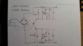
The last 4 tappings to the +ve side Zero volts and the last 4 tappings to the -ve side Zero volts, must all meet at a star point.
You then need to take a single wire to the junction of the smoothing capacitor and from that junction another single wire to the Centre tap of the transformer.
Electrically this layout looks identical to what your sch shows. The difference becomes apparent when you assign values of Impedance to every wire in your sch. The performance will be very inferior and that's why I said it won't work.
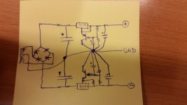
Thanks for pointing that out, the layout in my schematic is bad in regard to grounding. It was hastily scribbled down during breakfast... I'll hand in a proper version later.
No, it doesn't work.
The last 4 tappings to the +ve side Zero volts and the last 4 tappings to the -ve side Zero volts, must all meet at a star point.
You then need to take a single wire to the junction of the smoothing capacitor and from that junction another single wire to the Centre tap of the transformer.
Electrically this layout looks identical to what your sch shows. The difference becomes apparent when you assign values of Impedance to every wire in your sch. The performance will be very inferior and that's why I said it won't work.
How do we change this if we add a follow-up shunt circuit after it? Let's say an Active Regulator, does the Star Ground point on the right remain the new Star Ground, is there a new one or is there an additional one?
the post126 diagram becomes the Source of power for the next circuit/receiver.
Connect the source to the receiver using a twisted triplet.
Design the receiver circuit to minimise it's own loop areas.
Look carefully at that post126 diagram.
The transformer is connected to the rectifier with a triplet, make it a twisted triplet.
The rectifier is connected to the first smoothing bank with a twisted triplet.
The smoothing bank is connected to the regulator with a twisted triplet.
The regulator output is a twisted triplet.
All the inter module connections are twisted triplets.
That's the effective way to minimise interference.
That's why I said
If you were to try designing a PCB layout to match the performance of the hardwired version, you must take equal care to minimise the interference effect of the loop areas. The traces between the modules must be laid out to minimise the radiation of emi.
That is achieved by placing the flow and return traces adjacent to each other, or one above the other if a multi layer board.
Connect the source to the receiver using a twisted triplet.
Design the receiver circuit to minimise it's own loop areas.
Look carefully at that post126 diagram.
The transformer is connected to the rectifier with a triplet, make it a twisted triplet.
The rectifier is connected to the first smoothing bank with a twisted triplet.
The smoothing bank is connected to the regulator with a twisted triplet.
The regulator output is a twisted triplet.
All the inter module connections are twisted triplets.
That's the effective way to minimise interference.
That's why I said
YES !
If you were to try designing a PCB layout to match the performance of the hardwired version, you must take equal care to minimise the interference effect of the loop areas. The traces between the modules must be laid out to minimise the radiation of emi.
That is achieved by placing the flow and return traces adjacent to each other, or one above the other if a multi layer board.
Last edited:
the post126 diagram becomes the Source of power for the next circuit/receiver.
Connect the source to the receiver using a twisted triplet.
Hey Andrew, how's it going in Scotland?
Thanks for the tips, I think I got it, makes sense.
For the 'twisted triplets', you meant the wires in a P2P build, right?
I did my current prototype with proto board and some wires, I used the components legs as much as possible underneath it.
Will take these tips into account as I was planning to do some PCB during the holidays, nothing fancy, just perhaps some etching.
Looks like the layout sure can cause large variations in the circuit's performance, I think I even read they could "make or break" the performance.
Today I tested some additional small caps on a pair of toggles. I do get more high-range output out of it, but the highs appear quite unnatural and there's a hardness to them, not quite the glare of computer noise USB, but something else.
traces on a PCB can rarely replicate the efficiency of a twisted pair, which are excellent at tolerating emi and give a characteristic impedance if HF needs such.
Traces should try to achieve the tolerating qualities of the twisted pair.
Place the Flow and Return pair very close together, or one above the other on a thin substrate. Have you had the chance to examine the B.Putzeys' layout of his balanced volume control?
It is very easy to just copy the layout of a schematic without thinking about loop areas.
Get this (LOOP AREA) wrong and not only will it degrade measured performance, it can in the extreme break the circuit (oscillation).
traces on a PCB can rarely replicate the efficiency of a twisted pair, which are excellent at tolerating emi and give a characteristic impedance if HF needs such.
I like my Twisted pairs: I get great results with them (some DIY USB cable prototypes, my DIY SET Tube Amp, DIY Speaker cables). The other day I was thinking about this and PCBs which are usually layers of 2D layouts, no easy way of doing a proper TP.
However, with modern 3D printing techniques, we may be able to actually print a TP on new PCBs, 3D layer by 3D layer, this is probably be a game-changer when/if it happens.
Not yet, will check out what he came up with, although I'd be learning towards implementing my own Arduino + optical volume control. For now, I am looking at the active regulation/regulator and capacitor interactions for my Linear Regulator PSU as I am injecting clean power into the DAC and not the computer USB power anymore - astounding changes in SQ.Have you had the chance to examine the B.Putzeys' layout of his balanced volume control?
Looks like it's as important in the micro-view as the macro-view where ground loops can wreak havoc on the overall sound. Will explore that as well, thanks.Get this (LOOP AREA) wrong and not only will it degrade measured performance, it can in the extreme break the circuit (oscillation).
Actually, I already have a tab open from last night with a video of transient analysis and loop stability for regulators. Might need to do some mods in the workshop first before having the time to watch it though.
Last edited:
LM317 sense line + set resistor to case
BTW, do you know the answers to these two questions which popped up in my explorations?:
1. The recommended set resistor soldered to "case" - does it mean it is absolutely necessary to solder one end to the case itself, or is a soldering to the output enough to reach the same results (we know out is linked to case internally)? Also read about having two wires to the case (lower impedance)?
2. If I add the active regulation circuit post the regulator, what happens to our former regulator's sense line, we lose this ability, right? Can we do the same (another sense line) for the active circuit add-on?
Last edited:
Can we do the same (another sense line) for the active circuit add-on?
Only include a pcb trace (or wiring) in the sense loop, not any circuitry.
Only include a pcb trace (or wiring) in the sense loop, not any circuitry.
The question is: if I add the active reg after the LM317 (for which I know I can have a sense line when it's on its own), how is a sense line implemented if at all possible?
- Do we keep the same sense line as before? (doesn't seem sensible to me)
- Do we have a new sense line? (If so, where?)
- Is it in fact, not possible anymore for the end load
If I follow Andrew's star-grounding principle of considering the new active reg as the circuit for the reg, then the sense line can be from the reg but to the active reg, but I'm not sure that the best way to do it, since in the end, we're powering a load (in this case, my DAC).
I have seen a post by ALW if I remember correctly, pointing out how the proper sense line and sense return connection is very important when using a pre-reg as well as an active reg.
It looks like it is good to have a sense line from the pre-reg (in my case the LM317) to the active-reg output.
However, it isn't clear to me what the +ve sense line is nor how it is connected. I think I can get the GND sense line connection done though.
It looks like it is good to have a sense line from the pre-reg (in my case the LM317) to the active-reg output.
However, it isn't clear to me what the +ve sense line is nor how it is connected. I think I can get the GND sense line connection done though.
It is very easy to just copy the layout of a schematic without thinking about loop areas.
Get this (LOOP AREA) wrong and not only will it degrade measured performance, it can in the extreme break the circuit (oscillation).
OK, I think I understand how to minimise this loop area from the LM317, the adjust connections, the cap around the lower divider resistor as well as the output caps, with one star point for these. Then I can use this point to connect straight to the Load Return for the -ve sense line as well.
What do do with the tiny cap at the input of the LM317 though? Do I also connect its lower pin to the star point above (and additionally not to the bulk cap star point prior to it, correct)?
The input side cap is just to maintain a defined lowish impedance at higher frequencies. As the datasheet indicates, if you have a power supply cap nearby then no need for that extra cap. As such, that input cap can connect to 0V anywhere upstream of the 0V star you have.
Why do you want another reg after the 317 reg ???
Why do you want another reg after the 317 reg ???
Last edited:
As such, that input cap can connect to 0V anywhere upstream of the 0V star you have.
OK, so it wouldn't be good to connect it to the ref post-regulator, right?
Why do you want another reg after the 317 reg ???
For lower noise floor.
- Status
- Not open for further replies.
- Home
- Amplifiers
- Power Supplies
- LM317 experiments and measurements