You have 2 unity gain stages.
Just remove RV1 10k and remove R1
then jumper C4
then you will just have 2 unity gain stages in a row which is all it is anyways.
Vref half supply or virtual ground will be coming from the first opamp.
Why mute with a relay, just mute the input with a basic switch.
or mute with guitar volume knob.
Just remove RV1 10k and remove R1
then jumper C4
then you will just have 2 unity gain stages in a row which is all it is anyways.
Vref half supply or virtual ground will be coming from the first opamp.
Why mute with a relay, just mute the input with a basic switch.
or mute with guitar volume knob.
The intention was to have the hpf switch between the unity gain stages to keep the impedance high.
As for the relay, I want to avoid the DC pop on my cab, so having a timed mute delay stops that. It still pops regards of the guitar being connected or not as output cap hasn't had time to charge up at turnon.
As for the relay, I want to avoid the DC pop on my cab, so having a timed mute delay stops that. It still pops regards of the guitar being connected or not as output cap hasn't had time to charge up at turnon.
What you want to achieve is to avoid or minimize effects of the output on the input.Thank you @AIM65.
I see why the Zobel would get connected to power, but why would the others? Not disputing, Just wondering.
I thought anything in the Audio Path would require them to go to signal ground.
Would it also be wise to remove that 100 ohm resistor as the cap is already tied to the ground with that relay config?
From a pcb routing perspective, in audio frequency domain, that means to avoid or minimize effects of high current path of the output on the input side. First thing to do is to ensure that input side ground path are not shared my output side ones, in which flows high currents. That’s a consideration of pcb routing, and it doesn’t necessarily appear on the schematic. But if you want to make that appears on the schematic, you define two grounds (as you did) and explicitly connect them at a single point located on the pcb (with the net_tie) or even on the supply with a star based grounding scheme.
Here's a sketch which shows where high currents flows : supply rail, output of amp and the payload: the speaker. Speaker and supply should share the same ground distinct from the input one but connected in a single point, usually close to the power supply. Same for the Zobel even if it draws much less current tan the speaker. The relay as no effect as this is DC current. The 100 Ohms could be removed, but you should install 10 Ohms between pin 4 of relay and power gnd, rather than a direct connection.

Thank you so much 👍👍 as I'm redesigning it I'll take a deep look into it and come back if I have queries. Thank you
One more query for now. I have the regulator on a separate board to the amplifier. Would it be ok to have the PSU schematic components on the same board as the amplifier or would this introduce more noise or issues?
Yes, it’s ok, everything is DC and it’ll be cheaper.
Some lasts comment:
The amplifier will be boxed, this is not a lab thing, so you can remove the diode and use only one big ecap on the 36V rail, located close to the LM1875. SMPS doesn’t like being loaded by big cap, in case of trouble you can provision a 0.1Ω-2W resistor on the pcb in place of the diode. If ok, short it, if smps oscillate or can’t start, install it.
The divider and their cap should use Audio gnd, not Power gnd.
On the Zobel, don’t use a metal film resistor, they’re fragile, use a thick film 1W
With 10Ω to gnd on pin 4 of the relay, set your 555 monostable to at least 2s delay.
What’s the purpose of D2 close to the 555 ?
Thanks @AIM65 . Ive had a pretty big flare up with my chronic fatigue to its taken me a while to get this together.
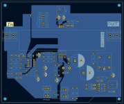
Does this look better?
Ive attached the Schematic I've redone and also the front and back of the pcb copper layers. I think it's alot better, but with my brain being a bit mushy at the moment theres a chance I might have missed something.
Does this look better?
Ive attached the Schematic I've redone and also the front and back of the pcb copper layers. I think it's alot better, but with my brain being a bit mushy at the moment theres a chance I might have missed something.
I just noticed this. Is this for all of the dividers & their caps?The divider and their cap should use Audio gnd, not Power gnd.
Attachments

Hi,
I hope you are recovering.
Some comments on the schematic :
I'll review pcb later. But the power tracks (the ones in red and blue on my previous sketch) are too narrow, make them wider.
Chris
I hope you are recovering.
Some comments on the schematic :
- C13 should be 100pF, not 10,
- 2W for R5 is enough,
- use carbon for R6, not metal film, this resistor can take up to 3.5A peak,
- the two lower parts of the dividers (resistor and cap) should be connected to GND_Audio_Input. That's because they set the bias of the amplifier, every signal or parasitic on those wires will be amplified by the amplifier s (x1 for the two TL072, X16 for the LM1875)
- you don't need to have a 'GND_Audio_output', just connect speaker and Zobel to the 'GND_Power'.
I'll review pcb later. But the power tracks (the ones in red and blue on my previous sketch) are too narrow, make them wider.
Chris
Thank you @AIM65. Getting there, but its always a slow process.
Thanks for the explanation. Ive reattached the changes.
As for the Power Tracks, they are 45 mil / 1.15mm. I thought that would be output current is less than 1A and the power not much more. Happy to be wrong though 🙂
Thanks Again Chris
Thanks for the explanation. Ive reattached the changes.
- C13 was a typo on my end =/
- R5 is actually 1W. Yet again....Fatigue.
- Changed the dividers as per your comment.
- Consolidated the output ground into the power ground.
As for the Power Tracks, they are 45 mil / 1.15mm. I thought that would be output current is less than 1A and the power not much more. Happy to be wrong though 🙂
Thanks Again Chris
Attachments
Hi,
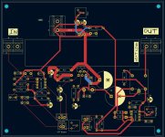
Usually, on a 2 layers pcb, tracks are on one side, gnd plane is on the other side with the few tracks that could not be routed on the other. Problem is that the gnd plane should not be interrupted by tracks, but when you have to, you have to think about where current flows inside the plane. This is true in audio frequency, but different in HF.
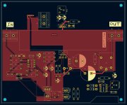
On your front side (blue) there’s an issue with the gnd plane in the red oval. The green arrows show the return current flow from the speaker. You have a high current path flowing through the very narrow piece a copper into the red oval. To fix this purpose, extend the gnd plane to the top border of the pcb. It’ll be better, even if not optimal.
You have the same issue with the yellow oval and to ground connection to C5 and C9 which are also high current. For minimal changes to your layout, implement bridges with a cluster of vias following the grey lines. An example of bridge is attached; the vias and red tracks connect the green ground plan, which is interrupted by a fat green vertical track.
In addition, you can remove the +36V track under the black cross and route it according to the pink line, and don’t forget to widen the high-power tracks, at least 3 mm. Move the nettie close to the negative pole of J2: speaker.
On your back side, widen the high-power tracks;, under certain circumstance current may reach LM1875 current limit between 4 and 5A.
Chris

Usually, on a 2 layers pcb, tracks are on one side, gnd plane is on the other side with the few tracks that could not be routed on the other. Problem is that the gnd plane should not be interrupted by tracks, but when you have to, you have to think about where current flows inside the plane. This is true in audio frequency, but different in HF.
On your front side (blue) there’s an issue with the gnd plane in the red oval. The green arrows show the return current flow from the speaker. You have a high current path flowing through the very narrow piece a copper into the red oval. To fix this purpose, extend the gnd plane to the top border of the pcb. It’ll be better, even if not optimal.
You have the same issue with the yellow oval and to ground connection to C5 and C9 which are also high current. For minimal changes to your layout, implement bridges with a cluster of vias following the grey lines. An example of bridge is attached; the vias and red tracks connect the green ground plan, which is interrupted by a fat green vertical track.
In addition, you can remove the +36V track under the black cross and route it according to the pink line, and don’t forget to widen the high-power tracks, at least 3 mm. Move the nettie close to the negative pole of J2: speaker.
On your back side, widen the high-power tracks;, under certain circumstance current may reach LM1875 current limit between 4 and 5A.
Chris
Attachments
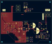
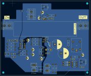
Ok Feeling much better about this! Can the 2 ground planes be too close together and cause "Pollution" of the signal ground?
You'll see 2 zones (C18 and C20) where i changed the fill to solid as I couldn't get the thermal pads, but they are overlapping and connected to the input ground.
This has been a great learning experience @AIM65 and i feel much better with the guidance you've given.
You'll see 2 zones (C18 and C20) where i changed the fill to solid as I couldn't get the thermal pads, but they are overlapping and connected to the input ground.
This has been a great learning experience @AIM65 and i feel much better with the guidance you've given.
Attachments
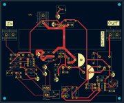
You're getting close the time you'll submit your order to the pcb factory !
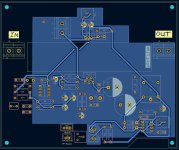
The path U2/pin4 -> R9 - > C9 -> K1 -> J2 must use wide tracks, this is a high current path.
That probably require you to shift right C6 & C5 and shift C9 down/left.
I do not like the loop U4/pin2 -> C19. C19 should be close to U4. Route +36V track to J4 below U4 not above, It'll free some space to set a short connection between U4 and C19.
You can also slightly shift right power ground plane below LM1875 in order to cover only power pins : 3,4 and 5. Pins 1 and 2 are input ones and could be covered by the signal ground, or nothing. The illustration below shows a signal ground plane on the left and a power one on the right.

And to finish, make the very narrow tracks wider. Narrow tracks are fragile and as it is DIY, tuning and rework are common... 🙂
If you're interested in pcb design, for DIY, read the paper attached. Author is Dave Jones from EEVblog. Content is very useful and practical.
Regards,
Chris
I don't think, but honestly I don't know. I usually use a minimum clearance of 0,5 mm.Can the 2 ground planes be too close together and cause "Pollution" of the signal ground?
The path U2/pin4 -> R9 - > C9 -> K1 -> J2 must use wide tracks, this is a high current path.
That probably require you to shift right C6 & C5 and shift C9 down/left.
I do not like the loop U4/pin2 -> C19. C19 should be close to U4. Route +36V track to J4 below U4 not above, It'll free some space to set a short connection between U4 and C19.
You can also slightly shift right power ground plane below LM1875 in order to cover only power pins : 3,4 and 5. Pins 1 and 2 are input ones and could be covered by the signal ground, or nothing. The illustration below shows a signal ground plane on the left and a power one on the right.
And to finish, make the very narrow tracks wider. Narrow tracks are fragile and as it is DIY, tuning and rework are common... 🙂
If you're interested in pcb design, for DIY, read the paper attached. Author is Dave Jones from EEVblog. Content is very useful and practical.
Regards,
Chris
Attachments
Hi
This resistor is used to load the cap at power up without shorting the LM1875 output. It will handle a lot of energy during a short period of time. I did some check before answering you using the datasheet of a random standard carbon resistor :
A Yageo CFR100 is a basic 1W carbon film resistor. According to DS, It can handle pulses of 1W during 1s or 100W during 100us, or 4W during 200ms.
At power up, the 2200uF, may face up to 36V step (worst case) through the 10Ω resistor resulting in a 3.6A current, 130W peak and more than 100W during approximately 2.4ms…That will destroy the resistor.
It’s better to use a 200 Ω - 1W and set the delay of the 555 to at least 1,5s.
Don't use a random value, it has influence on the output cap loading delay and then on the 'pop' sound in the speaker you're trying to avoid.
Sorry for the late response. Thank you 🙏 it's all working well, except for popping when it's turned off. Obviously the relay is not discharging quick enough but I'm not sure what I could change.
Hi
Great news !
Could you share pictures ?
Regarding the 'pop' sound, the circuit around the relay is designed to avoid pop at power on only , not power off !.
But there's a trick you can try, I'll sketch you something later.
Great news !
Could you share pictures ?
Regarding the 'pop' sound, the circuit around the relay is designed to avoid pop at power on only , not power off !.
But there's a trick you can try, I'll sketch you something later.
I don’t get how your 555 delay works. At power up, 555 should be triggered by a negative edge on TRG pin, but the circuit only provides a rising edge… does it really work ?. Does the trimmer position have an influence on the relay switch on delay ?. Usually, power up delay circuits with 555 looks like this one :
https://electronics.stackexchange.com/questions/353112/delay-turn-on-circuit-using-555
If you want power on and power off protection, the circuit become more complex. Feasible without 555, with some transistors.
ie:


At 0.00 this is power on; at 4.00 this is power off. Relay is On when Vrelay is low
This has not been tested, only simulated.
if you want to keep the 555, use the circuit described in the link above and part of the circuit above : Z1...T1..T2 then connect VF2 to the RESET pin of the 555 and also to a 10k pull up to +12.
https://electronics.stackexchange.com/questions/353112/delay-turn-on-circuit-using-555
If you want power on and power off protection, the circuit become more complex. Feasible without 555, with some transistors.
ie:
At 0.00 this is power on; at 4.00 this is power off. Relay is On when Vrelay is low
This has not been tested, only simulated.
if you want to keep the 555, use the circuit described in the link above and part of the circuit above : Z1...T1..T2 then connect VF2 to the RESET pin of the 555 and also to a 10k pull up to +12.
- Home
- Amplifiers
- Chip Amps
- LM1875 Noise