Originally posted by linuxguru After playing around in LTSpice for while, I came up with another nested gainclone concept similar to Walt Jung's composite op-amp/buffer.
Have you tried in LTSpice using WJ's multiloop concept putting a chipamp at the output?
I mean something following the original Jung's values:
http://waltjung.org/PDFs/WTnT_Op_Amp_Audio_4.pdf
My idea had been to replace the output chip for an LM3886, but I am not sure if they are unity-gain stable.
linuxguru said:
In the sims, the LM1875 can be used below the recommended gain of 10 with suitable compensation. However, I'm not sure that it extends all the way to a gain of 2. For unity gain or similar operation, the TI/Burr-Brown OPA549 family may be more useful, since they're unity-gain stable.
I did read that comment on the OPA549 being more suitable for that unity gain job, and in fact the 3886 datasheet advises a minimum of x10 closed loop gain.
So it looks as if the Jung concept might not be applied if using that chip.
So it looks as if the Jung concept might not be applied if using that chip.
another member says it's possible to stabilise the 3886 down to 3times. But, he did not specify the phase margin.
I worry that stability considerations for "nesting" slow, high minimum stable gain, power chip amps in effective multiloop amps are non-trivial
Jung's multiloop examples all use much faster output amps such that the input op amp's dominant pole compensation is fine for the whole loop since the fast output amp doesn't contribute very much phase shift at the unity loop gain intercept
with power chip amps you can't afford any extra phase shift at their (GBWmin )/ (Min stable gain)
that means that the input op amp's contribution to the outer loop gain must be flat from way below that frequency to >4x the power chip amp's max GBW/min stable gain
on the lower side this can mean you have to roll off the input op amp's gain to 0 dB near 20KHz - meaning your nesting isn't able to improve the power amp's behavior at or beyond that frequency
some have relied on the power amp never being worse than the typical spec on GBW - not a safe practice for diy builders without oscilloscopes and some knowledge of how to test for stability
I have built several multiloop amps with fast output devices – the most “powerful chip amp” I’ve used for the output is the LT1210 – but with its typical op amp Vsupply limits it wouldn’t go far with 8 Ohm loads
I would look for faster power amps – anyone know the GBW min spec for TDA729x DMOS chip amps?
Re: As a fly on the wall
Things might get a bit expensive if you do. The LM12 is far from cheap.
mwmkravchenko said:Anyone think about the LM12 as an output device?
Things might get a bit expensive if you do. The LM12 is far from cheap.
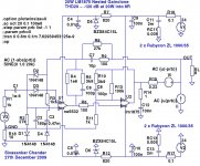
I had put this on the back-burner for a few months, and then took another look at it over the last week. I added a lifted ground and tweaked the compensation schema for better stability, and the THD20 is even lower and mostly even-harmonic. It now looks good enough to build a prototype.
A few notes on the schematic below:
1) Vi and Ii are injection sources using the Tien-Vishwanathan method for the open-loop gain simulation plots only. In the real circuit, Vi is a short and Ii is open.
2) R6 is required for the simulation to converge quickly - it's the equivalent of a base-stopper in discrete topologies.
3) The outer-loop gain and compensation is set by R8, R9 and C7.
4) The inner-loop gain and compensation is set by R4, R5 and C6. C6 is not very critical - any value above 22pF seems to work fine, with increasing stability (as well as THD) as C6 is increased. The 33pF value shown is a good compromise; higher values like 47 pF or 68 pF can be attempted on the first prototype for improved stability.
5) THD20 simulates at ~ -130 dB at 20W into 8 ohms, with a unity-gain phase margin of ~85 degrees.
6) No Boucherot/Zobel network is required.
Attachments
Little suggestion,
I don't like high impedance feedback circuits. Lower a bit the impedance of feedback circuits to decrease noise (main reason), DC offset and possibly THD (because input currents are highly nonlinear). Also, R1 could be lower to decrease noise. Besides, nice work, keep going 🙂
Cheers,
Nesa
I don't like high impedance feedback circuits. Lower a bit the impedance of feedback circuits to decrease noise (main reason), DC offset and possibly THD (because input currents are highly nonlinear). Also, R1 could be lower to decrease noise. Besides, nice work, keep going 🙂
Cheers,
Nesa
I had put this on the back-burner for a few months, and then took another look at it over the last week. I added a lifted ground and tweaked the compensation schema for better stability, and the THD20 is even lower and mostly even-harmonic. It now looks good enough to build a prototype.
A few notes on the schematic below:
1) Vi and Ii are injection sources using the Tien-Vishwanathan method for the open-loop gain simulation plots only. In the real circuit, Vi is a short and Ii is open.
2) R6 is required for the simulation to converge quickly - it's the equivalent of a base-stopper in discrete topologies.
3) The outer-loop gain and compensation is set by R8, R9 and C7.
4) The inner-loop gain and compensation is set by R4, R5 and C6. C6 is not very critical - any value above 22pF seems to work fine, with increasing stability (as well as THD) as C6 is increased. The 33pF value shown is a good compromise; higher values like 47 pF or 68 pF can be attempted on the first prototype for improved stability.
5) THD20 simulates at ~ -130 dB at 20W into 8 ohms, with a unity-gain phase margin of ~85 degrees.
6) No Boucherot/Zobel network is required.
Looks like very good work.
Have you tried simulating it driving any capacitive loads, just for fun? I played around with a lot of nested/composite amp simulations, a while back, but could only find models for some of the OPA5xx chipamps (e.g. OPA541E), at the time, unfortunately. By the way, for driving capacitive loads (with square waves, for example), it seemed that what was mainly needed was a lot of excess current-dumping capability, which I obtained, back then, by simply paralleling several of the chipamps.
Another interesting thing to try is using a spice model of a speaker, for the load, connected with a spice model for a speaker cable. I found some models for cables and speakers at Loudspeaker Cable Characteristic Impedance .
Eventually, I also added a power supply and star grounding to the simulations, and also modeled the resistances and inductances of the wires and PCB traces (particularly the ground returns), and the parasitics of the passive components.
P.S. If you would like an easy way to develop spice models for power transformers, from simple measurements, I have posted it here: Spice Component and Circuit Modeling and Simulation .
Last edited:
Thanks for all the comments.
@blueskynis: If the feedback network impedance is lowered, the input resistance to LGND also needs to be lowered to match it and null out the output offset voltage. About the lowest practical value of the feedback resistance here is about 10k. I tried it in the sim, and it made no significant difference to the sonics or stability, so no harm done.
However, lowering the feedback resistor uncovered a DC operating point latch-up issue - there's a small amount of hysteresis in the circuit due to the lifted ground. It didn't show up earlier with the 27k resistance, but kicked in at about 22k and saturated the output to ~ +/- Vsupply. I fixed it in the sim by adding back-to-back diodes between the inputs of the NE5532.
@gootee: I tried a small capacitive load in parallel with RL - the circuit remained stable up to about 220 nF, but became unstable at around 470 nF. I fixed it by adding some lead compensation around the LM1875 and modifying some of the earlier compensation networks. I also added an optional Boucherot cell to the output of the LM1875 - but the stability seems largely insensitive to its presence.
With these changes, it remains stable in small-signal conditions with a capacitive load of up to 2 uF in parallel with the 8 ohm load. However, at full output amplitude, the current limit kicks in on the LM1875 and the resulting output waveform is no longer sinusoidal at 20 kHz - it's distorted but still completely stable and free of any superimposed HF oscillations.
I'll try out the speaker, transmission line and transformer models in due course - thanks for the suggestion and the links.
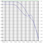
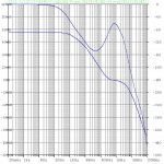
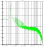
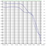
Here is the modified simulation schematic with the compensation changes, loop gain plot with a resistive 8 ohm load, and loop gain plot with a reactive 8 ohm || 2 uF load. It's barely stable in the latter case. The compensation changes also result in trading off about 10 dB of THD20, but it's still pretty good at -120 dB and the improved stability is worthwhile.
Edit: Paralleling several identical chipamps to increase the current-dumping capability is a simple and good idea, it just didn't occur to me. With the 0.22 ohm damping resistance at the output, there's no problem in summing the currents on the load side of the damping resistance.
@blueskynis: If the feedback network impedance is lowered, the input resistance to LGND also needs to be lowered to match it and null out the output offset voltage. About the lowest practical value of the feedback resistance here is about 10k. I tried it in the sim, and it made no significant difference to the sonics or stability, so no harm done.
However, lowering the feedback resistor uncovered a DC operating point latch-up issue - there's a small amount of hysteresis in the circuit due to the lifted ground. It didn't show up earlier with the 27k resistance, but kicked in at about 22k and saturated the output to ~ +/- Vsupply. I fixed it in the sim by adding back-to-back diodes between the inputs of the NE5532.
@gootee: I tried a small capacitive load in parallel with RL - the circuit remained stable up to about 220 nF, but became unstable at around 470 nF. I fixed it by adding some lead compensation around the LM1875 and modifying some of the earlier compensation networks. I also added an optional Boucherot cell to the output of the LM1875 - but the stability seems largely insensitive to its presence.
With these changes, it remains stable in small-signal conditions with a capacitive load of up to 2 uF in parallel with the 8 ohm load. However, at full output amplitude, the current limit kicks in on the LM1875 and the resulting output waveform is no longer sinusoidal at 20 kHz - it's distorted but still completely stable and free of any superimposed HF oscillations.
I'll try out the speaker, transmission line and transformer models in due course - thanks for the suggestion and the links.
Here is the modified simulation schematic with the compensation changes, loop gain plot with a resistive 8 ohm load, and loop gain plot with a reactive 8 ohm || 2 uF load. It's barely stable in the latter case. The compensation changes also result in trading off about 10 dB of THD20, but it's still pretty good at -120 dB and the improved stability is worthwhile.
Edit: Paralleling several identical chipamps to increase the current-dumping capability is a simple and good idea, it just didn't occur to me. With the 0.22 ohm damping resistance at the output, there's no problem in summing the currents on the load side of the damping resistance.
Attachments
Last edited:
P.S. If simulating with a square-wave input, it makes sense to band-limit the input, to set a defined maximum slew-rate for the edges of the square waves, unless you're just looking for potential high-frequency instabilities, or want to see what happens when you try to exceed the chipamp's maximum slew rate.
It is discussed, and the calculations needed are given, in the thread at the following link:
http://www.diyaudio.com/forums/solid-state/117469-square-wave-testing-slew-rate.html
For a final product, it also makes sense to add RF filtering at each amplifier's input (and output, and power supply connections). See Section 7 of Walt Jung's "Op Amp Applications Handbook", which is on line in its entirety, for free, at:
ADI - Analog Dialogue | Op Amp Applications Handbook
Cheers,
Tom
Last edited:
@gootee: Thanks for the links - I'll try out the square-wave and slew rate tests in due course.
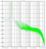
Meanwhile, I managed to stabilize it further - the tweaked compensation in the schematic shown below allows it to drive a 10 uF || 8 ohm load stably. The output waveform stays sinusoidal up to about 200 mW output, after which the LM1875 goes into current-limiting and the waveform becomes more or less triangular. In any event, it does not show any HF instability, either before or after current limiting sets in.
The tradeoff? Another ~10 dB of THD20 has to be given away, taking it to about -110 dB - it's still worthwhile, IMHO.
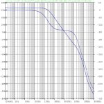
Shown below is the modified simulation schematic including the 8R || 10 uF load, the loop gain plot with the 8R || 10 uF load, and the output waveform FFT plot at 200 mW into 8R || 10 uF.
Meanwhile, I managed to stabilize it further - the tweaked compensation in the schematic shown below allows it to drive a 10 uF || 8 ohm load stably. The output waveform stays sinusoidal up to about 200 mW output, after which the LM1875 goes into current-limiting and the waveform becomes more or less triangular. In any event, it does not show any HF instability, either before or after current limiting sets in.
The tradeoff? Another ~10 dB of THD20 has to be given away, taking it to about -110 dB - it's still worthwhile, IMHO.
Shown below is the modified simulation schematic including the 8R || 10 uF load, the loop gain plot with the 8R || 10 uF load, and the output waveform FFT plot at 200 mW into 8R || 10 uF.
Attachments
@gootee: Thanks for the links - I'll try out the square-wave and slew rate tests in due course.
Meanwhile, I managed to stabilize it further - the tweaked compensation in the schematic shown below allows it to drive a 10 uF || 8 ohm load stably. The output waveform stays sinusoidal up to about 200 mW output, after which the LM1875 goes into current-limiting and the waveform becomes more or less triangular. In any event, it does not show any HF instability, either before or after current limiting sets in.
The tradeoff? Another ~10 dB of THD20 has to be given away, taking it to about -110 dB - it's still worthwhile, IMHO.
Shown below is the modified simulation schematic including the 8R || 10 uF load, the loop gain plot with the 8R || 10 uF load, and the output waveform FFT plot at 200 mW into 8R || 10 uF.
Very nice!
Have you looked at it in the time domain, with a (slew-rate-limited) square wave? I bet that with some paralleled chipamps, it could do nice square waves into a significant amount of PURE capacitance (although you might also need a small inductor and parallel resistor before the output).
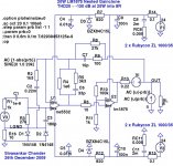
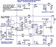
Nested Howland gainclone
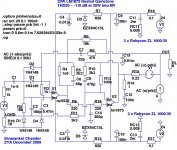
Here's the next iteration of the nested gainclone topology, this time with (sort of) paralleled chipamps at the output. After seeing the Inguz and the Mauro Penasa topologies, I went with the Howland Current Pump (improved version) at the output for several reasons:
1) Compensation is easier.
2) Great stability into capacitive loads - it's a current source at the output.
3) Both the non-inv and inv- inputs of the chipamp see signals that are similar in phase, so the character of the dominant pole in the chipamp isn't that critical. It's easier to substitute chipamps and expect it to work without trouble.
4) It's fairly easy to parallel chipamps at the output for increased drive capability - it only involves adding currents.
The attached schematic is fairly straightforward, with the possible exception of the compensation network between the op-amp and the chipamp. The inner chipamp (2 x LM1875) is a Howland Current Pump, with one master and one slave which simply supplies higher current drive capability. The outer feedback loop (R10, R3) is simply a Walt Jung-style voltage series feedback loop around the NE5532 outer opamp, which is itself set for a gain of ~(1 + 150/1) by R4 and R16.
C7 is part of a modified Deboo integrator for the Howland CP - in the textbook case, one end of C7 would have been grounded. However, it makes no difference to the Howland if that end is connected to a compensation network (in this case, R5, R8 and C6). This allows 3 loops to be compensated together, with just 4 passives:
1) C7 itself is a Deboo integrator (lag compensation for the chipamp).
2) C7-R5 lead-compensates the NE5532 (just incidental, and mostly unnecessary).
3) In addition, C7, R5, C6 and R8 also form a 2nd-order lead-compensation network for the outer feedback loop (note that the voltage at the non-inverting input of the chipamp is mostly a scaled version of the voltage at the output of the chipamp, and the phase information is still available after scaling).
(A simpler (1st-order) version of this compensation network is simply a series-connected resistor and capacitor between the non-inv input of U2 and the junction of R16-R10. It works fine, but the phase of the loop-gain plot gets a kink, which is easier to straighten out with the 2nd-order network shown).
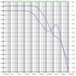
At 22V output amplitude into 8R (about 30W), THD20 is about -106 dB, almost entirely even-harmonic. H3 is almost 38 dB below H2.
From the loop gain plot, The phase margin is about 100 degrees at unity loop-gain, and the phase of the loop-gain stays rather flat from 20 kHz to 300 kHz.
(The simulated results seem to indicate parity in all metrics with the Mauro Penasa MyRef Rev C, but arguably better distortion and sonics. With some minor tweaks, it is conceivable that a 2 x LM3886 output stage can be substituted for the 2 x LM1875, allowing output power in excess of 100W.)
Here's the next iteration of the nested gainclone topology, this time with (sort of) paralleled chipamps at the output. After seeing the Inguz and the Mauro Penasa topologies, I went with the Howland Current Pump (improved version) at the output for several reasons:
1) Compensation is easier.
2) Great stability into capacitive loads - it's a current source at the output.
3) Both the non-inv and inv- inputs of the chipamp see signals that are similar in phase, so the character of the dominant pole in the chipamp isn't that critical. It's easier to substitute chipamps and expect it to work without trouble.
4) It's fairly easy to parallel chipamps at the output for increased drive capability - it only involves adding currents.
The attached schematic is fairly straightforward, with the possible exception of the compensation network between the op-amp and the chipamp. The inner chipamp (2 x LM1875) is a Howland Current Pump, with one master and one slave which simply supplies higher current drive capability. The outer feedback loop (R10, R3) is simply a Walt Jung-style voltage series feedback loop around the NE5532 outer opamp, which is itself set for a gain of ~(1 + 150/1) by R4 and R16.
C7 is part of a modified Deboo integrator for the Howland CP - in the textbook case, one end of C7 would have been grounded. However, it makes no difference to the Howland if that end is connected to a compensation network (in this case, R5, R8 and C6). This allows 3 loops to be compensated together, with just 4 passives:
1) C7 itself is a Deboo integrator (lag compensation for the chipamp).
2) C7-R5 lead-compensates the NE5532 (just incidental, and mostly unnecessary).
3) In addition, C7, R5, C6 and R8 also form a 2nd-order lead-compensation network for the outer feedback loop (note that the voltage at the non-inverting input of the chipamp is mostly a scaled version of the voltage at the output of the chipamp, and the phase information is still available after scaling).
(A simpler (1st-order) version of this compensation network is simply a series-connected resistor and capacitor between the non-inv input of U2 and the junction of R16-R10. It works fine, but the phase of the loop-gain plot gets a kink, which is easier to straighten out with the 2nd-order network shown).
At 22V output amplitude into 8R (about 30W), THD20 is about -106 dB, almost entirely even-harmonic. H3 is almost 38 dB below H2.
From the loop gain plot, The phase margin is about 100 degrees at unity loop-gain, and the phase of the loop-gain stays rather flat from 20 kHz to 300 kHz.
(The simulated results seem to indicate parity in all metrics with the Mauro Penasa MyRef Rev C, but arguably better distortion and sonics. With some minor tweaks, it is conceivable that a 2 x LM3886 output stage can be substituted for the 2 x LM1875, allowing output power in excess of 100W.)
Attachments
I'm impressed. My own sim trials with TinaTi were quite disappointing. Obviously their opamp models weren't ment for distortion analysis.
Did you do a reality check by simulating simple circuits with various gains and loads?
I'm curious what THD20 a simple LM1875 might have with gain of 10 and a 4 ohm load?
regards
Did you do a reality check by simulating simple circuits with various gains and loads?
I'm curious what THD20 a simple LM1875 might have with gain of 10 and a 4 ohm load?
regards
This will likely not work. The second LM1875 (U3) is operating at unity gain, but they are not stable at unity gain, they require a gain of 10 or higher for stability. You might be able to externally compensate it but I don't see anything like that in your schematic. I think that U3 will oscillate resulting in high current between it and U2 through RZ1 and RZ2.Here's the next iteration of the nested gainclone topology, this time with (sort of) paralleled chipamps at the output. After seeing the Inguz and the Mauro Penasa topologies, I went with the Howland Current Pump (improved version) at the output ....
The unity-gain buffer is stable in the sim, and I expect it to be fully stable when constructed. Note that the global negative feedback loop (which includes the unity-gain buffer) is fully compensated with ~100 degrees phase margin at unity loop-gain. If you break the GNFB loop, the buffer may oscillate, but that probably won't happen unless you overdrive the chipamps into hard clipping.
Note also that the Mauro Penasa gainclone also operates its Howland Current Pump at fairly low voltage gain, but it is nevertheless stable because of the compensation applied to the GNFB loop.
In any event, it's easy to replicate the Howland CP including the negative feedback network and eliminate this issue if necessary. The non-inverting input of both Howlands will then be driven from the (common) Deboo integrator node. I don't believe this is necessary, but I'll simulate it in due course.
- Status
- Not open for further replies.
- Home
- Amplifiers
- Chip Amps
- LM1875 nested Gainclone