I have posted 12 previous comments/advices in this thread. (~50% contribution of all comments offered.)
To date you have ignored the majority of that content and gone your own way.
I have invested much time in your project, but it appears to be a waste, I give up.
To date you have ignored the majority of that content and gone your own way.
I have invested much time in your project, but it appears to be a waste, I give up.
Last edited:
go back and read the 12 previous posts and what the other 12 replies had to offer.
Hi AndrewT,
May be this time i have understand & implemented the correct type.🙁
Attachments
much better.
Hopefully others will come in and comment.
Thanks.
Any improvenents required?😎😎
Thanks Again
One Silly Question..
what if i use 2200/63v cap of 30 mm dia??
Further others are requested to give their input.
Thanks
what if i use 2200/63v cap of 30 mm dia??
Further others are requested to give their input.
Thanks
Peter Daniel uses fairly high value decoupling capacitors in his designs. This allows him to delete all the smoothing capacitance from the PSU and still give him adequate performance.
Hi Neeraj
That last layout in post 46 is starting to look good.
The power supply decoupling is really nicely done now.
There's still a couple of problems though:
First, there's a 470uF capacitor that looks like it went in by mistake.
Also the Zobel network (2.7R, 0.1uF) should be connected to power ground, not signal ground.
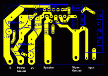
I've changed the layout a bit and attached a picture to show what I mean.
I'm not sure how you want to organize the grounding.
You might need extra "Power Ground" connections on the PCB because all the following need to be connected together somehow:
A) "Power Ground" on the PCB
B) 0V on the power supply
C) The loudspeaker return wire
D) The chassis
E) Safety earth
I included a "Signal Ground" connection but you probably don't need it. The "Signal Ground" is often just connected to the "Power Ground" on the PCB with a 10R resistor, and not separately connected to the chassis. This works well but then the "ground" terminal of the input socket must be connected to the chassis where it is mounted.
Cheers - Godfrey
That last layout in post 46 is starting to look good.
The power supply decoupling is really nicely done now.
There's still a couple of problems though:
First, there's a 470uF capacitor that looks like it went in by mistake.
Also the Zobel network (2.7R, 0.1uF) should be connected to power ground, not signal ground.
I've changed the layout a bit and attached a picture to show what I mean.
I'm not sure how you want to organize the grounding.
You might need extra "Power Ground" connections on the PCB because all the following need to be connected together somehow:
A) "Power Ground" on the PCB
B) 0V on the power supply
C) The loudspeaker return wire
D) The chassis
E) Safety earth
I included a "Signal Ground" connection but you probably don't need it. The "Signal Ground" is often just connected to the "Power Ground" on the PCB with a 10R resistor, and not separately connected to the chassis. This works well but then the "ground" terminal of the input socket must be connected to the chassis where it is mounted.
Cheers - Godfrey
Attachments
Hi Neeraj
That last layout in post 46 is starting to look good.
The power supply decoupling is really nicely done now.
There's still a couple of problems though:
First, there's a 470uF capacitor that looks like it went in by mistake.
Also the Zobel network (2.7R, 0.1uF) should be connected to power ground, not signal ground.
I've changed the layout a bit and attached a picture to show what I mean.
I'm not sure how you want to organize the grounding.
You might need extra "Power Ground" connections on the PCB because all the following need to be connected together somehow:
A) "Power Ground" on the PCB
B) 0V on the power supply
C) The loudspeaker return wire
D) The chassis
E) Safety earth
I included a "Signal Ground" connection but you probably don't need it. The "Signal Ground" is often just connected to the "Power Ground" on the PCB with a 10R resistor, and not separately connected to the chassis. This works well but then the "ground" terminal of the input socket must be connected to the chassis where it is mounted.
Cheers - Godfrey
Hi Godfrey🙂
The PCb layout looks more neat & clean then drawn by me.
As per AnderwT & Carlos FM's Schematic
1. Connect Cz to Power Ground.
2. Rz is connected to Speaker Out from Chip
3. 470uF capacitor is intentionally put there to block DC( As recomended by AndrewT)
Hi,
what is the problem with using a 470uF NFB cap?
The RC in conjunction with 100r is 47ms.
The input filter (2u2F & 15k) is 33ms.
These values seem compatible.
But I do see a problem with the Rin value and the NFB values.
Neeraj has +IN seeing 15k33 to ground. The source is blocked by a capacitor
The -IN sees 2k0 to ground. the 100r is blocked by a capacitor.
This will introduce extra and avoidable output offset.

🙂 I'm taking forever to do mine. Waiting on some capacitors ordered from overseas at the moment.
Any chance of a schematic or an assembly diagram in more readable colours than yellow on white? 🙂
Looks good to me, for what that's worth. 🙂 You could thicken a few tracks dramatically or use polygon fills to cover over zig-zags (dog-legs) but I can't see that it would make a lot of difference.
Good luck!
Hi random007,🙂🙂🙂
Sorry for my delayed reply.😱
1. Schematic is in Post#1
2. Ya can print in black also ( its on Express PCB)& i am doing the same on eagle free version also if you need i can mail so that you can modify to suit your need.
Thanks on your input.


1. Opps. Kind of obvious. 🙂Hi random007,🙂🙂🙂
Sorry for my delayed reply.😱
1. Schematic is in Post#1
2. Ya can print in black also ( its on Express PCB)& i am doing the same on eagle free version also if you need i can mail so that you can modify to suit your need.
Thanks on your input.
2. That's OK, I'm about done with mine. I'm very appreciative that people on these forums have pointed out some basic mistakes in my crazy designs and given me a better understanding of RC filters, to name a few things of the many I've been learning.
Good luck!
After reading all this talk about the 3886, I'm still left wondering where I would find a well-designed pcb to build one of these amps?
I purchased a pair off ebay (already built) and could not eliminate the hum and noise from the outputs. I am guessing at this point that they were not designed well, possibly including poorly-implemented ground planes and/or lack of star grounding.
I purchased a pair off ebay (already built) and could not eliminate the hum and noise from the outputs. I am guessing at this point that they were not designed well, possibly including poorly-implemented ground planes and/or lack of star grounding.
- Status
- Not open for further replies.
- Home
- Amplifiers
- Chip Amps
- LM 3886 PCB Based On Carlos Fm Schemetic