I am no expert.
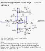
But there aren't any differences between that circuit diagram and any other basic lm3886 i have built so far.
except i didn't bother with R4 , R5, C7, C8
MY personal minimum suggestion for c2 and c4 for 8 ohm load is 4700uF but 2200 will probably also do. Depending what size you have on the powersupply. side.
One person says the feedback resistor should be big 200k and higher and next person say feedback resistor should be small, you will have to experiment.
one person says use carbon film resistors , the next person say metal film has better properties and the 3rd guy will say anything less than dale or military spec gives crap sound and you are wasting your money if you don't use them.
my 2 cents 🙂
Hi Tangmonster,
Thanks for reply.😀
Yes the load is 8Ohms & the cap on PS Side is 24700mfd/rail (10000X2, 4700X1)
that too is based on Carlos schematic.
2nd Option PCB is attached 😎😎
Thanks for reply.😀
Yes the load is 8Ohms & the cap on PS Side is 24700mfd/rail (10000X2, 4700X1)
that too is based on Carlos schematic.
2nd Option PCB is attached 😎😎
Attachments
Last edited:
that Carlos schematic includes all the options, except the DC blocking cap in the NFB loop.
That means that any output offset generated inside the chipamp will be multiplied by the gain of the amp, i.e. about 21times.
In addition the resistance seen by the -IN input is 2k//100r ~95r.
The +IN input sees 15k+330r ~15330r.
This difference in input source resistances will give a higher output offset and the resulting offset will vary more with chip temperature than if the resistances matched.
If you are using Carlos amp with Carlos PSU, then stick with his capacitor values, except if your experimentation proves that improved performance is obtained by doing otherwise.
Next, do not read all the Ground symbols as being the same. They are not the same.
The ground at the bottom of the 15k (R1) is the Signal Return. Connect this with it's Signal Hot as a twisted pair to the RCA input socket.
The ground at the end of 100r (R2) is also signal referenced. Connect it to the bottom of R1. these are the Signal Ground. Never mix Signal Ground with Power Ground through a common trace/wire.
Connect top of C3 to bottom of C5 directly by the shortest possible route, even soldering the two pins together.
Connect top of C2 to bottom of C4, using a short trace.
Connect C3/5 to C2/4. This is Power Ground.
Connect C7 to Power Ground.
Connect C8 to Power Ground.
Connect Cz to Power Ground.
Connect Power Ground to your Main Star Audio Ground.
Connect Signal Ground to Main Star Audio Ground.
Connect Speaker Return to Main Star Audio Ground.
Connect Chassis to Main Audio Star Ground.
Connect Protective Earth (the third wire in the mains cable) to the Chassis.
Last edited:
Hi AndrewT,
Thanks for reply.I am bit confused with
1. Connect top of C3 to bottom of C5 directly by the shortest possible route, even soldering the two pins together.
2. Connect top of C2 to bottom of C4, using a short trace.
Please Explain.
Do you mean 2000+.1uf or 0.1+0.1uf Please go through PCB lauouy & guide.
Last edited:
Hi,
the decoupling capacitors meet the very short term current demand of the amplifier.
They can only do this if the total route length from +ve power pin to -ve power pin through the decoupling capacitors is VERY SHORT.
Any wasted length adds to trace/route inductance and reduces the ability of the decoupling to meet instant current demand.
The slower transients that are fed from the electrolytic can tolerate some trace/route inductance and so the electrolytic route can be longer. The long term current demand is met by the PSU capacitors and since they are at the far end of the PSU connecting cables the inductance in this long routes does little harm. That is, provided you have made allowance for the decoupling to properly meet the short term demands of the amplifier.
Back to
The next part is the length of the route through the cap, i.e. pin to pin. Keep the cap pins VERY SHORT. Use a small capacitor with close pitch pins (2.5mm is better than 5mm, is far better than 10mm).
Then the route from +ve cap to -ve cap, soldering the pins together is the shortest possible route. Then through the -ve cap and finally to the -ve pin.
This total route from +v to -ve power pins must be VERY SHORT for the ceramic or MKT capacitor. MKP and FKP are physically too big.
the decoupling capacitors meet the very short term current demand of the amplifier.
They can only do this if the total route length from +ve power pin to -ve power pin through the decoupling capacitors is VERY SHORT.
Any wasted length adds to trace/route inductance and reduces the ability of the decoupling to meet instant current demand.
The slower transients that are fed from the electrolytic can tolerate some trace/route inductance and so the electrolytic route can be longer. The long term current demand is met by the PSU capacitors and since they are at the far end of the PSU connecting cables the inductance in this long routes does little harm. That is, provided you have made allowance for the decoupling to properly meet the short term demands of the amplifier.
Back to
The route from the +ve pin to C3 must be VERY SHORT. Some builders solder the cap pin directly to the +ve pin.Connect top of C3 to bottom of C5 directly by the shortest possible route, even soldering the two pins together
The next part is the length of the route through the cap, i.e. pin to pin. Keep the cap pins VERY SHORT. Use a small capacitor with close pitch pins (2.5mm is better than 5mm, is far better than 10mm).
Then the route from +ve cap to -ve cap, soldering the pins together is the shortest possible route. Then through the -ve cap and finally to the -ve pin.
This total route from +v to -ve power pins must be VERY SHORT for the ceramic or MKT capacitor. MKP and FKP are physically too big.
Last edited:
Hi AndrewT,🙂
Thanks for your guidance.Will implement the same on PCB Layout.
What is the suggested value of DC blocking cap in the NFB loop.
I have mounted the 0.1MKT directly on 2200 uf ( solderside of PCB).
please suggest the best suited PCB Layout.
Thanks for your guidance.Will implement the same on PCB Layout.
What is the suggested value of DC blocking cap in the NFB loop.
Back to The route from the +ve pin to C3 must be VERY SHORT. Some builders solder the cap pin directly to the +ve pin.
I have mounted the 0.1MKT directly on 2200 uf ( solderside of PCB).
please suggest the best suited PCB Layout.
I calculate the NFB cap as follows.
NFBcap >= 1.4 * Cin * Rin / Rfb
where:
Cin is the DC blocking cap at the input.
Rin is the resistance to ground following Cin that sets the high input filter
Rfb is the lower leg NFB going to ground.
For Carlos schematic
1.4 * 2u2 * 15k / 100 = 467uF.
Cnfb >=467uF so that the input filter sets the LF bandwidth of the amplifier and reduces distortion brought about by having an AC voltage across the NFB cap.
I calculate the NFB cap as follows.
NFBcap >= 1.4 * Cin * Rin / Rfb
where:
Cin is the DC blocking cap at the input.
Rin is the resistance to ground following Cin that sets the high input filter
Rfb is the lower leg NFB going to ground.
For Carlos schematic
1.4 * 2u2 * 15k / 100 = 467uF.
Cnfb >=467uF so that the input filter sets the LF bandwidth of the amplifier and reduces distortion brought about by having an AC voltage across the NFB cap.
Hi AndrewT,
thanks for your reply.
Is 470 uf Non polar will do work.
Let me know about the pcb layout.
thanks
Hi,
is this another question?
Do posts 4, 8 & 10 spell out my recommendations in detail?
You choose whether to accept or reject some or all of those suggestions.
is this another question?
Do posts 4, 8 & 10 spell out my recommendations in detail?
You choose whether to accept or reject some or all of those suggestions.
Andrew
Have you ever considered a career in the Diplomatic Service?
There are ways of making points and then there are ways....... Not everyone is as switched on about electronics as you seem to be and English may not be his first language.
Neeraj, Andrew is doing an exact calculation for the NFB cap based on Carlos's FM's circuit values. 467 uF is not a standard value for an electrolytic cap so the closest higher value (470 uF) is fine. They probably have a tolerance of -10%/+20% anyway so you can always up the value slightly by paralleling with say 47 uF to allow for that or just leave it at 470 uF. It won't make that much difference either way..
Last edited:
they would never have me.Andrew
Have you ever considered a career in the Diplomatic Service?
I keep putting my foot in my mouth, Sometimes I spot it and delete my opinion.
Sometimes my opinion slips out even when it is hurtful.
For those occasions where I have inadvertently hurt someone, I appologise.
But there are some/many lazy buggers that expect us to do all the work. They refuse to read before posting. They refuse to read the post. They refuse to do any homework. I cannot tolerate these Members and unfortunately I voice that opinion as well.
If you ever get the chance to meet me, you will find I am a nice guy who is tolerant of all and understands that everyone is entitled to hold an opinion.
Just this Forum thing seems not to suit certain human frailties and I fall into that category.
Sorry to all, except the lazy buggers that refuse to research their project.
Andrew
My observation was more tongue in cheek than anything.
I know what you mean though. I often wonder if some of the people contributing here should be let anywhere near a soldering iron, let alone lethal mains voltages.
If they don't know exactly what they're doing they should go out and buy it. It'll be a lot cheaper in the end a lot less hassle. Good quality kit doesn't cost a fortune these days.
Last edited:
hello AndrewT.....
you seems very familiar with this gainclone or "chip-amp" stuff,
I wonder, by your years of experience with these chip-amps....
are they really worthed for us to take it seriously,
since in my past experience, I think gainclone is a nasty beast which is really hard to tame.....
It's seems impossible to get those separated dimensional sounds, just like the original gaincard.....
And when people claim to tame their gainclone by having sweet music from their amps, I think what they hear is their fancy hi-end resistors/capacitors setup which they use in their amps....
thx in advance,
regards🙂
Invain - what really matters with Gainclones is that you use them within their capabilities i.e:
1. no 4 ohm speakers so current limiting doesn't activate
2. limited power output to avoid clipping, which requires higher than average sensitivity speakers
Don't forget that these chips have output stages with limited current capability and protection circuits which are audible when activated. If you try to run an LM3875 loudly into 4 ohm, 84dB/1W sensitivity speakers it will sound terrible.
The power supply is important too. Some advocate low capacitance supplies which supposedly favours mid/treble purity at the expense of bass slam. Others go the other way. Carlos FM's snubbered supply takes what he thinks is the best compromise route.
THE CHOICE IS YOURS. My advice would be to bi-amp with an LM3875 running off a low capacitance (1500-2200uF) supply for the mid/treble driver and an LM3886 with a Carlos FM PSU (maybe regulated) for the bass. In my opinion that gives you the best of both worlds.
Forget about boutique resistors and caps. They have a second order effect only. I can almost feel the flames from here after saying that!!
Last edited:
Invain,
I basically agree with Gopher.
Use the limited current capability of any of the chipamps, wisely.
One can only do that if one researches the topic and develops a specification/target/outcome that is SMART. The A of SMART is Achievable and the R is Realistic.
I basically agree with Gopher.
Use the limited current capability of any of the chipamps, wisely.
One can only do that if one researches the topic and develops a specification/target/outcome that is SMART. The A of SMART is Achievable and the R is Realistic.
Neer,
look at your PCB layout.
Measure the length of the direct route from +ve supply pin to -ve supply pin.
Now measure the decoupling route on your PCB from +ve pin to plastic cap, across the cap pins, along the power ground track to the other plastic cap, across the -ve cap pins and finally to the -ve supply pin.
Compare the short route to the long route!! These should both be very short. If you are using 0.2inch pin pitch caps then the long route should be ~0.5 to 0.8inches. If you use 0.1inch pin pitch caps, then the long route should be <0.4inches.
Look at the power input connections at the edge of the PCB.
How do you minimise the current loop of the +ve supply and the power ground?
How do you minimise the current loop of the -ve supply and the power ground?
These three wires should arrive at the PCB as a twisted triplet to minimise loop area and the three tracks from the edge connections to the main current client (the +ve & -ve supply pins) should run parallel and very close to each other, again to minimise the loop area.
Last edited:
- Status
- Not open for further replies.
- Home
- Amplifiers
- Chip Amps
- LM 3886 PCB Based On Carlos Fm Schemetic