Hello!
I recently bought three pairs of LJM amp kits, the MX50SE, L7, and NAP250mod.
All are working, no smoke at startup, no oscillations etc. Power supply is +-37V and has a pair of beer can-size Philips capacitors.
However I noticed what must be crossover distortion on one of the L7 boards. Sound is not clean when played on a really low volume. Since it has no series resistors with the output drivers, it's not easy to measure bias current, but I'm pretty sure that must be the issue.
I would like to add a pot to adjust it, and referring to schematic in post 541 in this thread, trimpot could be instead of R12 or R13, right?
However in my amps i have no '601' transistors, Q11 is a 5551. PCB has a panda logo, so it should not be too old.
Link to post 541 with schematic.
https://www.diyaudio.com/forums/vendor-s-bazaar/180625-ljm-audio-55.html#post4844361
I will probably add trimmers to adjust the MX50SE bias too, just for peace of mind.
Hope somebody can confirm the bias trimpot, and maybe a smart way to measure bias with no resistors?
Last edited:
However in my amps i have no '601' transistors, Q11 is a 5551. PCB has a panda logo, so it should not be too old.
Can't edit my post, so forget this statement, missed the marking on it..
Does anyone know where I can get a Schematic diagram for L-20D having some trouble with the kit from ebay.
Hello!
Hope somebody can confirm the bias trimpot, and maybe a smart way to measure bias with no resistors?
U can use current clamp meter
or
put a 100R/2W in series with one the DC V supplies
calculate the current: V = i/r
L7 simulation
does anyone know where I can find the .asc file of the LJM L7 scheme for simulation with ltspice or ngspice?
does anyone know where I can find the .asc file of the LJM L7 scheme for simulation with ltspice or ngspice?
Hi to all fellow members and friends.
I am interested to build two of Class D amps as kits. The available PS I have has + - 56 VDC. Looking at L20D specs, there is a note that min power supply is 60 VDC but at L15D the max is 60 VDC close to my PS voltage. The question:
Can I chose and operate the L20D with + - 55VDC?
If not, is it safe to use L15D with this voltage?
Thanks in advance for your kind attention and help.
Regards,
John
L15D should be fine with +-56 volt if you don´t push it to the limit or use extremely low load resistance. Your usual PS will drop under load, so maybe even without signal you will have "real" 55V, depending on the VA the transformer has
.
.
Thanks Ivan.
Take care, the pinout of the CC5551 is not pin compatible with the 1N5551
The CC5551 has collector on the centre pin (ECB) whereas the 1N5551 is EBC
I'm not sure which post you are replying to but I expect that you mean 2N5551 rather than 1N5551? Certainly the pinouts of 2N5551 and CC5551 are different but CDIL's datasheet shows BCE for CC5551 and EBC for 2N5551 - That is, when viewed normally from the label side with the leads pointing downward.
It seems that only CDIL make this variant and it's an oddball, so I would avoid it, otherwise I'd forget and it would become a source of error and confusion if used in other projects too.
It seems that only CDIL make this variant and it's an oddball, so I would avoid it, otherwise I'd forget and it would become a source of error and confusion if used in other projects too.
Last edited:
Replacing CC5551 with 2N5551
Yes, the CC5551 used in LJM kits is a bit of an oddball.
The 2N5551 is not pin compatible with the CC5551 although they are otherwise very similar. There is however a variant of the 2N5551 with centre collector called the 2N5551-C but that too isn't easy to find.
I suspect the centre collector variant was used to simplify the PCB layout.
I'm not sure which post you are replying to but I expect that you mean 2N5551 rather than 1N5551? Certainly the pinouts of 2N5551 and CC5551 are different but CDIL's datasheet shows BCE for CC5551 and EBC for 2N5551 - That is, when viewed normally from the label side with the leads pointing downward.
It seems that only CDIL make this variant and it's an oddball, so I would avoid it, otherwise I'd forget and it would become a source of error and confusion if used in other projects too.
...I noticed what must be crossover distortion on one of the L7 boards. Sound is not clean when played on a really low volume.
I observed the same with all of my 4 boards of the L7 at low output signal (@ 1W into 4 Ohms or less). I am using +/- 42V supply voltage.
THD decreases with increasing output power and/or increasing idle current, indicating crossover distortion as the predominant cause.
Above 1kHz THD is rapidly increasing to relatively high 0.2-0.3% at 20 kHz if the amp output power is 1W or less. This is actually too much for a decent design. Also IM-distortion is high at low output power. When the output power is increased, both, THD and IM decrease. The distortion at low output level is particularly strong for the frequency range between1 kHz and 20kHz, barely detectible for frequencies of 1 kHz and less.
The bias divider resistors are 9.1k/10k. In the early series the divider pair was 10k/11k instead. Care must be taken not to swap them, because then idle current goes through the roof and the amp says good bye with fire and smoke (unless prevented by proper fuses in the rail voltage lines, strongly recommended). Small changes in the resistor values have huge effect on the bias current here, therefore I do not recommend a trim-pot for bias adjustment here. I guess, That's why also LJM put fixed resistors instead.
I figured out, that with the bias divider 9.1k/10k the heat sink remains pretty cool, LTSpice simulation indicates a very low idle current of few milliamps at best and shows crossover distortions in the >10kHz sinus output. THD for 10kHz at 1W into 4 Ohms was about 0.2-0.3% while for 1 kHz it was 0.1%.
I increased the 9.1k bias divider resistor to 10k (to exactly the same value as the 2nd bias divider resistor) carefully matching both to less than <1% difference. This resulted in about 30mA idle current through each of the power-MOSFETs and gentle warming of the heat sink (without load).
Additionally, I increased NFB by reducing the 33k NFB resistor to half (16.5 kOhms) - by adding a 2nd 33k in parallel. This cuts the amplifier gain in half, of course. For me, the resulting gain of 14-15 is still more than sufficient.
Both measures together cut THD in half. THD for 10kHz @ 1W into 4 Ohms load went down to <0.1% and at 10W/4 Ohms to about 0.06%. Crossover distortions at low output power are mostly gone. THD is now slightly increasing with increasing output power as one would expect.
At 10W/4Ohm and higher, THD in the 20Hz-1 kHz frequency range remains < 0,01%. For 8 Ohms load it's even better.
Another approach to reduce crossover distortion is matching the MOSFET power transistors. I noticed that for one of my four L7 amp modules, THD was considerably smaller (40% less) than for the other three. I didn't measure/match the IRFP240/IRFP9240 pairs (simply used what was in the DIY kits). I assume, that in this "better" module, the match of the MOSFET pair happened to be better by chance.
Regards,
Reinhard
Re. L7 amp crossover distortion (THD) at low output
I wrote above:
"Above 1kHz THD is rapidly increasing to relatively high 0.2-0.3% at 20 kHz if the amp output power is 1W or less."
I should have written: "THD...at least 0.2-0.3%, even up to 1% THD at 1W (or lower output)." Therefore, the improvement in THD by increasing the idle current to 25-35mA and doubling negative feedback (putting 2nd feedback resistor with same value in parallel to the existing one) is minimum a factor of 2-3 but can be by a factor of 5-7 for higher frequencies (1-20kHz).
Another bullet point:
Several members in this forum reported blown L7 modules.
Here my thoughts on it.
If run under moderate operating conditions, the L7 is reliable. Moderate means that sine output shall not exceed 50W/4Ohms or 100W/8Ohms significantly or over a longer period of time. The L7 power modules are electrically capable to deliver more power, but not thermally. The L7 is definitively not suited for speaker impedance of <4 Ohms either.
What does that mean? There is an inherent physical limit for heat conductivity from the power-MOSFETs into the heat sink. The possible output power of the L7 at high supply voltage (i.e. 40V or more) easily exceeds the SOA (safe operating area) of the power MOSFETs, which is mainly determined by the finite heat conductivity from the transistor package to the heat sink and heat dissipation rate of the heat sink and specified in the transistor's data sheets.
For this reason, LJM recommends a large heat sink of min 0.5 kg per L7 amp module and 1kg size from 40V supply up. However, even that isn't doing the job well enough, if one tries to run it at high power, i.e. >50W into 4 Ohms or >100W into 8 Ohms, because one complementary output pair cannot quickly enough dissipate the heat for >50W into 4 Ohms continuously. As a result, the transistor die heats up too much, exceeds the max. allowed junction temperature.
From the MOSFET's datasheets it is not difficult to calculate that for 50W/4 Ohm a thermal resistance of about 0.5°C/W max. is required. That's what a large heat sink can typically provide. Thus, even if the heat sink is large enough the bottleneck of the heat conductivity from the transistor die (inside the transistor package) through the package, the silicone pads into the heat sink remains. And, simply said...it's this heat constraint why a single pair of power transistors can't deliver safely more than 50W continuous (sine) power into 4 ohms, even not with a large heat sink. For 100W it takes at least two pairs of power transistors per channel - just not to exceed the specified upper temp. limit of 150°C inside the power transistor.
Therefore, the claim (for L7) that 150W into 8 Ohms and even 300W into 4 Ohms were possible must be questioned.
Poor heat contact to the heat sink, too small heat sink or pulling too much power from the L7 (which unfortunately is easily done as the L7 does not include a limiter) are IMHO typical causes for blown L7.
Best Regards,
Reinhard
It's basic rule in amp design, when it goes more and more into class-A, that you have to split your output in more devices pairs. Even more if the transistors are plastic types, as I think I remember the LJM uses.
If you are so concerned about low level crossover distortion you should definitely add more MOSFETs. There's no way out for that one.
If you are so concerned about low level crossover distortion you should definitely add more MOSFETs. There's no way out for that one.
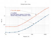
In the attachment you see the effect of the measures I described above. Actual THD measurements (for 1W into 4 ohm) match the LTSpice simulation results.
orange: L7 by LJM (original configuration with 33k NFB resistor and 9.1k/10k bias divider)
blue: L7 modified (2x33k NFB resistors in parallel and 10k/10k bias divider)
Regards
Reinhard
orange: L7 by LJM (original configuration with 33k NFB resistor and 9.1k/10k bias divider)
blue: L7 modified (2x33k NFB resistors in parallel and 10k/10k bias divider)
Regards
Reinhard
Attachments
No, not that circuit. That's not how my L7 looks. A bunch of resistors and one capacitor are different and of course, IRF610 as bias transistor.
I got the latest version of L7 and I checked the values in my model against it.
I am attaching the asc file for my circuit and the MOSFET models I used with it (from Ian Hegglun, June 2019) as well as the BJT models I used for 2N5401 and 2N5551. The two 0.01 Ohm resistors were added in the asc. for simulation only in order to monitor idle current.
Regards
Reinhard
My comments were based on (real) THD measurements primarily. The LTSpice model (asc. attached) could reproduce the measured data.
Attachments
Last edited:
Pls. replace the .asc by the updated one in my post above.
Are you familiar on how to get to THD in LTSpice?
1. You must first replace the (default) transistor models in your LTSpice library by the models I have attached.
2. Click on V(OUT) in the schematics to obtain the result in the time domain. If in your case node (019) is identical to V(out), that works also.
3. After the simulation in the time domain completed, right click on the window with the (green) sine curve result (it looks like the one you posted). Then a menu pops up. Go to "View..." in that menu and then to "Spice Error Log". Then the Spice Error Log window pops up.
4. In the Spice Error Log window scroll down to the table which lists the Fourier components of V(out). The last line reports the THD.
If you change frequency, you must do that in the .FOUR command as well as in the voltage generator parameter. The file as supplied by me has both at 20 kHz.
You may also want to change input voltage to obtain an output of 1W into 4 Ohm load. The file that I provided generates 9V peak into 4 Ohm, which corresponds to 6,3Vrms that makes 10W into 4 Ohm.
Last edited:
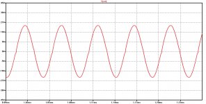
To start with, the asc file i'm using is yours, not mine. So that "green" image comes from your simulation. Forget my simulation.
What is the result I should get? Please run it on your LTSpice and capture the screen.
Second, I'm using your models.txt you enclosed, so the transistor models are yours.
The THD in the error log window is 0.0195%, which is good for 20K.
I didn't change anything. I'm running it as you sent it. The screen I get is from Vout.
You can also detect the crossover distortion in the (Cordell based) "L7" file that you have (the one you posted). Although that's not exactly L7, it shows the same characteristic high crossover distortions.
Check sine output for 20 kHz and zoom in.
You can easily spot it, even for high output in your simulation file THD = 1.3% at 20 kHz for 35W into 8 Ohm load. I used your file and here is the result.
Regards
Reinhard
Check sine output for 20 kHz and zoom in.
You can easily spot it, even for high output in your simulation file THD = 1.3% at 20 kHz for 35W into 8 Ohm load. I used your file and here is the result.
Regards
Reinhard
Attachments
Last edited:
- Home
- Vendor's Bazaar
- LJM Audio