AndrewT said:Hi Tony,
Sorry.
The double barrelled does indeed have coupled collectors below the cascodes. I had not picked that up in the simple two pair schematic.
The numbers stack up well for 2ohm.
8 quads can achieve 1kW @ 60degree phase angle and with Tc<100degC. Sink ~<90degC
This was some test for Bensen's SOA spreadsheet. I have never tried to do a cascaded output stage before.
I estimate that power from +-76Vdc with +-60mF per channel after you have biased it up. Iq=400mA from +-76Vdc Pq=61W. That will need a fairly big sink, but your going to have that just to fit 32 To3s in place.
hi,
i was thinking 400mA quiscient current too...
😀 can you point me to Bensen's spreadsheet please? thanks..
i just liked the sound of the super leach amp, and i was wondering how a really high powered version work out.
and jens, really glad to see that you are still on the ball...nice lay out, it keeps getting better... maybe we can have that input front-end option as separable from the output stage, no?
JensRasmussen said:Hi all,
A quick update:
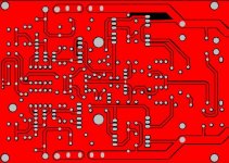
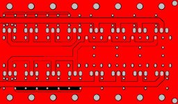
http://www.delta-audio.com/temp_jens/Super_Leach_ver_2.4_PCB.pdf
I changed the feedback, and consider getting rid of the large caps placed on the top of the board.
\Jens
Could you explain the feedback change?
Thanks
Hi Jens,
what about moving the hi current fuses and the PSU input terminals towards the output end and away from the voltage amp. The space created by deleting the BIG cap leaves lots of room.
Would it be possible to move the power input to the opposite end of the board?
what about moving the hi current fuses and the PSU input terminals towards the output end and away from the voltage amp. The space created by deleting the BIG cap leaves lots of room.
Would it be possible to move the power input to the opposite end of the board?
Would it be possible to move the power input to the opposite end of the board?
yes, that's on my mind too...
Hi,
I am using adobe reader 6.0 but I cannot read the different layers of the pdf file that Jens posted. What do I need to do so?
Tks
I am using adobe reader 6.0 but I cannot read the different layers of the pdf file that Jens posted. What do I need to do so?
Tks
Hi All,
Not much activity down here.
I just wish I could boost this thread a bit.
regards to all super leach'rs !
Not much activity down here.
I just wish I could boost this thread a bit.
regards to all super leach'rs !
Hi guys when you do a group buy let me know i will definitely be in for a few boards probably 10 or more. wow i cant wait for this to become a reality. looks awesome Jens.Keep up the great work everyone.
Cheers
Bowdown
Cheers
Bowdown
Leach superamp pcb
This thread began in February of 2005. I believe it to be a worthwhile project and would buy any number of boards to see it to construction. Many projects on the forum have been built in the 50-150 watt range. This particular, tried and true design, is in the power range many of us would like to own. How can we get this thing going so we can populate the boards. I currently do not have the resources or knowledge to do it, but am learning. Tad
This thread began in February of 2005. I believe it to be a worthwhile project and would buy any number of boards to see it to construction. Many projects on the forum have been built in the 50-150 watt range. This particular, tried and true design, is in the power range many of us would like to own. How can we get this thing going so we can populate the boards. I currently do not have the resources or knowledge to do it, but am learning. Tad

Hi bigpanda,
http://www.diyaudio.com/forums/showthread.php?postid=815584#post815584
but it looks like it is not anymore available.
send me your email and i'll send it to you.
http://www.diyaudio.com/forums/showthread.php?postid=815584#post815584
but it looks like it is not anymore available.
send me your email and i'll send it to you.
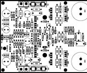
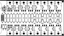
Hi,
I thought about how to get a PCB design made that enabled the builder to have either a two or one board layout depending on what heat sinks is on hand.
I came up with the idea of having solderpads that could either be used for wires while at the same time have the connections made in the PCB... if two boards are needed simply break the PCB in two and you have the output stage seperated from the input.
See the schematics.
\Jens
Attachments
- Status
- Not open for further replies.
- Home
- Amplifiers
- Solid State
- Leach Super Amp Pcb Re-Design (LSAPRD)