Got it. Thanks ZM.
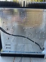
Spreader on SIT side mounted. I dressed the mounting side w 800 grit to knock down any small defects. Thin layer of thermal paste applied, torqued M4s to 1.2nM. Flying gate resistor inside the shrink tube is 47R. THF-51S mounted with correct Keratherm.

Spreader on SIT side mounted. I dressed the mounting side w 800 grit to knock down any small defects. Thin layer of thermal paste applied, torqued M4s to 1.2nM. Flying gate resistor inside the shrink tube is 47R. THF-51S mounted with correct Keratherm.
Last edited:

Proceeding to the Mu follower side.
Question - do I need insulated shoulder washers for the IXTN40P50P M4 screw mounts?
https://www.littelfuse.com/~/media/...osfets_p-channel_ixtn40p50p_datasheet.pdf.pdf
Question - do I need insulated shoulder washers for the IXTN40P50P M4 screw mounts?
https://www.littelfuse.com/~/media/...osfets_p-channel_ixtn40p50p_datasheet.pdf.pdf
No.
You can check it yourself by measuring resistance between the metal base and each of the G S S D terminals.
You can check it yourself by measuring resistance between the metal base and each of the G S S D terminals.
do I need insulated shoulder
no
metal tab is insulated from semi itself
you need nice washers though, in between screw heads and metal tab
do not forget split washers, too
Thanks Ben and ZM! Good copy on the hardware, I've got the split washers (M4 Bellevilles do not fit due to circumference limits) I will go ahead and add flat washers below.
Meanwhile:

Meanwhile:

none
entire circuit isn't possible to juice through bulb tester, current is too high
if you're going to test just PSU, clever, use whatever you have from 40W to 75W
entire circuit isn't possible to juice through bulb tester, current is too high
if you're going to test just PSU, clever, use whatever you have from 40W to 75W
^Thanks very much. PS tested perfectly, 71V. I don't have a Variac so will have to do a Luke Skywalker.
Reminds me to ask you: do I need to ground one side of the input, per schematic, or did you handle that in the PCB?
Reminds me to ask you: do I need to ground one side of the input, per schematic, or did you handle that in the PCB?
do I need to ground one side of the input, per schematic, or did you handle that in the PCB?
Maybe too late, as you did apply power
I'm Manuel regarding question above, please clarify
there is no offset, as you have output cap
what you need to set is output node voltage, inside end of coupling cap, say "C*" pad
what you need to set is output node voltage, inside end of coupling cap, say "C*" pad
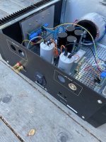
Well I hope I didn't damage anything. Let's circle back: Lower left of SIT/SET schematic in post #1 shows IN_GND connected to one leg of R1 and the other to GND. I have IN+ and IN_GND leads soldered to the input RCA, and a shorting device applied to the RCA jack. No other wires to ground.
Both trim pots were checked and set at mid-value before startup.
Both sinks made plenty of heat, no smoke / smells present.
If I read you correctly, you are saying read voltage at the C8 cap on the Mu PCB between C* and C**. What output node voltage shall I aim for, and how to adjust?
Both trim pots were checked and set at mid-value before startup.
Both sinks made plenty of heat, no smoke / smells present.
If I read you correctly, you are saying read voltage at the C8 cap on the Mu PCB between C* and C**. What output node voltage shall I aim for, and how to adjust?
I have IN+ and IN_GND leads soldered to the input RCA, and a shorting device applied to the RCA jack. No other wires to ground.
that's correct
Both trim pots were checked and set at mid-value before startup.
correct
Both sinks made plenty of heat, no smoke / smells present.
sounds good
If I read you correctly, you are saying read voltage at the C8 cap on the Mu PCB between C* and C**. What output node voltage shall I aim for, and how to adjust?
mild reminder :
(late) edit on Jan 25. 2024. - change of Mu resistors values, as per Ben Mah's suggestion - post #17, https://www.diyaudio.com/community/threads/lazy-singing-bush.388164/post-7069779
Tnx Ben
Knowing that you already did your homework regarding Mu resistor groups value, I didn't followed it further
So, I believe it can be carved in stone as 5*1R as upper group and 5*1R5 as lower ( puck source side) group
Mu pcb; put probes across R4 (practically having 0R2 there) and fiddle with P1 (10K) to get in vicinity of 640mV; means 3A2 Iq
then SIT pcb: put red probe on "C*" pad, black probe to GND (anywhere) and fiddle with P1 (5K) to set voltage approx to 1/2 of rail value; say that you have 60Vdc rail, so 30-ish Vdc is your goal
why I didn't name those 2 pots with different names?

Super helpful ZM. Cooking this morning, 10K P1 Mu trim maxxed out full CW = 580mV, 5K P1 SIT maxxed out = 32V, rails at 65V.
Are we close enough, or do we need to tweak?
Haven't connected a source signal or speaker yet.
Are we close enough, or do we need to tweak?
Haven't connected a source signal or speaker yet.
to get to 640mV across 0R2 group (3A2 Iq), decrease R1 (8K2)
back up with P1 on Mu pcb, sorta mid position, then replace said R1 with 3K3 to 5K1, whatever you have in drawers
32V on output node is right bingo
back up with P1 on Mu pcb, sorta mid position, then replace said R1 with 3K3 to 5K1, whatever you have in drawers
32V on output node is right bingo
- Home
- Amplifiers
- Pass Labs
- Lazy Singing Bush