

That U12 chip setup looks very similar to the F16 masked chips on the class D type 1 amps.
If so, then that chip may be MC14060
David
If so, then that chip may be MC14060
David
U12 is a MC14060B. Link Below. U14 is a LM361. Link Below.
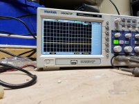
U12 is an squarewave oscillator.U12-Pin 5 feeds Pin 2 of U13-TL072C. Pin 1 of U13 feeds the base of Q103-3875GR. C266-47p at the base of Q103 integrates the squarewave and generates a triangle wave.
You should see a triangle wave at Pin 4 of U14 comparator. Pin 3-U14 is the signal or audio input. Pin 13-U14 should be the composite squarewave and audio.
If you have an oscilloscope look to see if you have the triangle and squarewave at the Pins I mentioned. Post screenshots. Also, measure the DC voltages around U14 using the negative speaker terminal for black probe and scope ground. Post the results in the following manner:
U14
Pin 1-
Pin 2-
Pin 3-
etc
https://www.onsemi.com/pub/Collateral/MC14060-D.PDF
http://www.ti.com/lit/ds/symlink/lm361.pdf
I just looked at Perry’s guide and Perry has notes on that very amp in the misc. stuff folder.
Maybe if you have his tutorial you can review his notes.
Oh. I see PapaZBill just found your post. You’re in good hands.
Maybe if you have his tutorial you can review his notes.
Oh. I see PapaZBill just found your post. You’re in good hands.
Last edited:
The circuit and all of the ICs are essentially the same as this JBL.
http://www.bcae1.com/temp/bp1200p1_sm.pdf
This is the green board version of the kicker.
Service manual, eprom result list | Elektrotanya
http://www.bcae1.com/temp/bp1200p1_sm.pdf
This is the green board version of the kicker.
Service manual, eprom result list | Elektrotanya
U14
pin 1) 11.69v
pin 2) 0v
pin 3) 1.73v
pin 4) 5v
pin 5) 0v
pin 6) -12.05v
pin 7) 0v
pin 8) 2.78v
pin 9) 0v
pin 10) -1.54
pin 11) 1.18v
pin 12) 0v
pin 13) 2.78v
pin 14) 2.78
pin 1) 11.69v
pin 2) 0v
pin 3) 1.73v
pin 4) 5v
pin 5) 0v
pin 6) -12.05v
pin 7) 0v
pin 8) 2.78v
pin 9) 0v
pin 10) -1.54
pin 11) 1.18v
pin 12) 0v
pin 13) 2.78v
pin 14) 2.78
Correction: I meant to say Pin 11 not Pin 13. Check for a squarewave at Pin 13. Also check Pin 4 for the triangle wave. If possible take a screenshot and post.


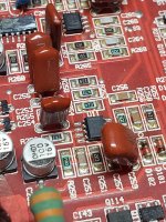
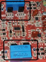
I posted your pic of main board, that's been cropped. Please take a close up of this area and post. I tried to magnify your pic, but not able to without pixalation. I will be able to edit pic and point out test points etc
The U14-LM361 may have failed. Replace if you haven't already. Also, check the DC voltages across D107,D108,D120,D121.
The U14-LM361 may have failed. Replace if you haven't already. Also, check the DC voltages across D107,D108,D120,D121.
Attachments

I will be replacing the lm361 and all of the cy and dy transistors tomorrow when the parts come. I will check everything in the box u outlined also.
I replaced the lm361 and all of the cy and dy transistors. all of the components in the box tested ok.
When I power up the amp without the output fets I'm getting positive and neg rail on the both outside fet leg pads of both the pnp and npn banks. When I put 1 fet in each bank the amp cycles in and out of protect rapidly. I dont know what the next step is or where to look
Not sure what you mean by pnp and npn banks. the terms are not relevant to Mosfet's. The cy and dy are BJT's and are npn and pnp transistors.
Each side has 3 banks-1 bank of 3 IRF640's and 2 banks of IRF9640's. You may be able to check the drive w/o any output's install or you must have at least one mosfet in each bank.
Each side has 3 banks-1 bank of 3 IRF640's and 2 banks of IRF9640's. You may be able to check the drive w/o any output's install or you must have at least one mosfet in each bank.
sorry. I meant n fets and p fets. When I put 1 fet in each bank the amp cycles in and out of protect. I was able to put 1 in each bank of one side and it powered up fine. Then I took them out and put them on the other side and it started going in and out of protect again.
- Home
- General Interest
- Car Audio
- kx1200.1 help