Cap
If this cap is big (like it is now) will it lead to HF roll-off? Today I ran a bunch of power tests and I think I noticed some HF attenuation.
If this cap is big (like it is now) will it lead to HF roll-off? Today I ran a bunch of power tests and I think I noticed some HF attenuation.
another cap
I found another cap 1500 pF that makes the amp stable at idle with no input.
This has no HF rolloff, but there is overshoot in the square wave. Only a small amount at 2KHz but a little more at 20 KHz.
What does this indicate- instability into different loads?
I found another cap 1500 pF that makes the amp stable at idle with no input.
This has no HF rolloff, but there is overshoot in the square wave. Only a small amount at 2KHz but a little more at 20 KHz.
What does this indicate- instability into different loads?
Re: another cap
I think it is more correct to say change in the gain/phase margin as the reactance in the load changes.lgreen said:there is overshoot in the square wave. Only a small amount at 2KHz but a little more at 20 KHz.
What does this indicate- instability into different loads?
The 3300pf cap gives a 3dB down point at about 14 KHz. The 1500pf cap moves that up to 25 KHz.
It sounds like it might be time to do as Phil suggested in post 356 and separate the VGS from the output. This will show which has the problem.
It sounds like it might be time to do as Phil suggested in post 356 and separate the VGS from the output. This will show which has the problem.
Steve Dunlap said:The 3300pf cap gives a 3dB down point at about 14 KHz. The 1500pf cap moves that up to 25 KHz.
It sounds like it might be time to do as Phil suggested in post 356 and separate the VGS from the output. This will show which has the problem.
Thanks.
I understand what trace to cut and where to put the resistor.
I don't get this sentence
then used the junction of the resistor, Q7 and Q10 as the input to the output stage.
this part I don't get? What goes where?
Also, since I am now using this cap, its not in the schematic right? Where would it be?
Also- my experiments indicate that after apply some real power to a real load, the sinks and transistors heat up and instead of having to have the bias set at the max, I can turn it down and still get 8-10 mV across the emitter resistors. Offset reduces to 150 mV after running for about 10 min at about 5W.
So this is something I may live with. -3db at >20KHz is ok with me.
The junction of Q7 and Q10 need a DC bias source. That is what the resistor Phil added was for. This gives an electrical common point between the non grounded end of the resistor and the junction of Q7 and Q10. You can use this end of the resistor to inject a signal to the output.
The cap (C2) is not on the schematic because I never used it on the amps I built. It was present on the commercial models. The cap connects the base to collector on Q4.
The cap (C2) is not on the schematic because I never used it on the amps I built. It was present on the commercial models. The cap connects the base to collector on Q4.
originally posted by Steve Dunlap
The 3300pf cap gives a 3dB down point at about 14 KHz. The 1500pf cap moves that up to 25 KHz.
thanks Steve. You saved me the trouble of a calculation that I haven't done in several years and would have to look up.
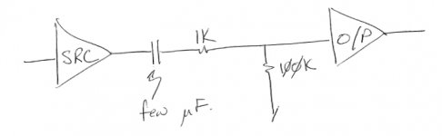
lgreen -- I've attached a sketch of what I mean. SRC is the signal source for the output stage, e.g., your signal generator. O/P is the Krill output stage. The junction of the 1k and 100K resistors is connected to the junction of Q7 and Q10, which is what I referred to as the input to the output stage.
The cap and two resistors in the sketch are not in the schematic and will go away once you complete trouble-shooting. So....
1. Cut the trace and add the 100K resistor (value not critical) from junction of Q7 and Q10 to ground.
2. Disconnect the power to the output stage but keep the AC power connected to the power supply for the VGS.
3. Go back to the VGS and check offset and oscillations without any compensation cap.
4. Correct any problems which will now be related to only the VGS or power supply.
5. Connect power back to output stage.
6. Put scope and DMM on output of the output stage. Check for offset, idle current and oscillations. You don't need the extra cap or 1K resistor for this step. You could also make same measurements with the 1K resistor as shown in the sketch but connecting the open end of the resistor to the ground. See if it makes any difference.
7. Correct any problems and adjust idle current.
8. Add the cap and connect signal generator to output stage as shown in sketch. Check response.
9. Connect VGS back to output stage but as shown in sketch where SRC is now the VGS.
10. Check everything again.
11. Remove 1k and 100K resistors and the new cap and connect VGS to output as shown in Steve's post 251 schematic.
About that 1500 pF cap... It's only masking the problem you're seeing, it's not fixing it. The circuit should work fine without it or with a small value (10 - 30 pF).
Attachments
Vgs
I don't know what you mean by the VGS- it is "voltage gain stage" but where is it? Q1 and Q2? where am I probing? The the base of Q2? R11?
let me see if I understand.
You are saying-
1. Cut the trace to Q7/Q10. the long stright one from Q6. cut vgs here.
2. Check the input stage at the output of R11 which is available and will have the same voltage as at the place where I just made the cut.
3. Adjust DC offset with R26 which operates on this part of the circ. Also that weird cap I have been using will effect this part of the circ. 3 pf should do it? (that is my only small value!).
4. Now check the output stage (connect power to it), you cut its input but not a big deal, you can run open circ, or with 1K to ground, so do both
5. Adjust bias on the output using R27. Look at the response. Watch out for oscillations.
6. Hook up the signal gen to the output stage, use a 1K and dc blocking cap in series with the sig generator directly into the cut made previously. Analyze response.
7. Hook up the input to the output, but not directly. Putting a DC blocking cap and a 1K into the cut trace in series, and a 100K to ground.
8. remove everything (the cap, 1K and 100K), reconnect the cut, and you are good to go?
Have I got this right?
So what you are saying is to cut the trace. To adjust the input part alone. To adjust the output part alone. To join the in to the out by using a dc blocking cap and resistors, and adjust that. And finally to remove everything and go back to where we started without the cut trace?
That sounds right. The output will need a resistor to ground when separated from the VGS (voltage gain stage) to prevent major DC offset. The 1K to ground should take care of this.
The purpose of this is to check and see witch part of the amp has a problem. The DC offset should be set after the two stages are reattached.
The purpose of this is to check and see witch part of the amp has a problem. The DC offset should be set after the two stages are reattached.
pcb cut
before dr. green does the operation- you are sure i have the right trace to cut?
(shown in the pic)
before dr. green does the operation- you are sure i have the right trace to cut?
(shown in the pic)
bogdan_borko said:Could anyone tell something about the "sound"?
I thought you have been living with the amp for the last two months - why do you need to hear other's opinion of the sound?
bogdan_borko said:I`ve done listening tests of krill for a two months now
Hi,jkeny said:
I thought you have been living with the amp for the last two months - why do you need to hear other's opinion of the sound?
he can't believe how good it sounds. He is looking for corroboration in case his ears are deceiving him.
operation
Ok, the good Dr. is going to operate!
After the patient is out, I'll make an incision on the trace shown in yellow to cut the trace. I'll use a dremel with a standard cutting disc to etch away the trace. I'll drill two holes shown in red. I'll run a wire (dotted line) from the junction of the output transistors on the bottom of the board to the 1st hole (on the left). Another wire (dotted line) will go on the bottom of the board from R11 up through the hole (on the right) to the top of the board.
Thus I'll have wires from R11 (output end I hope) and from the input end of the outputs passing from the bottom of the board to the top. When all is done I'll just connect the wires at the top of the board together. I could be more bold with the hole location but I am not sure the Dr.'s hands are so steady.
This will leave a small scar on the patient, but I hope he will not complain?
Any 2nd opinions? "do you concur?"
surgery plan
jkeny said:
I thought you have been living with the amp for the last two months - why do you need to hear other's opinion of the sound?
Because nobody said anything except me...

Enjoy the krill 😀
surgery complete!
Ok I have separated the voltage gain stage from the output statge, disconnected the high power PS and looked at the signals.
-I get a small 20uS oscillation (1 period) if an input is connected (50KHz?)
-this is present with the 1K and .1 uF cap on the input; with no RC on the input; with C2 = 5pF or C2 = 1500 pF.
-I get offset just like before but much lower 30mV to 150 mV and the control does not reduce offset, just increases it.
what next?
It sounds like you have the wrong value for R14. A 560 instead of a 56 will cause what you are measuring. Turn off the power and measure the resistor.
- Home
- Amplifiers
- Solid State
- Krill construction thread - 100W version