When doing layouts using KiCad, are there any guidelines that should be followed when routing traces?
Is there a preferred method of putting traces on---like power first, or maybe ground connections first?
Is there any disadvantage to using many vias?
Is there a preferred method of putting traces on---like power first, or maybe ground connections first?
Is there any disadvantage to using many vias?
Well, there are few hard-and-fast rules here for PCB layout design. It depends on the type of project you are doing (digital, analog, RF, etc.), the resources available to you (number of layers), and what has to go together onto the PCB.
Most of my projects are for hobbyist use and are intended to be inexpensive so these are restricted to two layer boards. In most cases, I will have at least one, sometimes both sides copper fill zones with ground. You can use many vias to stitch the bottom and top together. Vias tend to be inexpensive and structures like via fences can help provide low resistance/inductance ground returns as well as shield EMI. The only place where vias can be problematic is that too many of them can constrict traces or remove too much copper area from the ground plane, or in extreme cases weaken the PCB, especially with more advanced materials like Rogers microwave substrates (FR4 tends to be pretty robust as a whole). I usually default to 0.5 mm clearance for copper around holes/pades, but will increase this to 1.0 mm when voltages above 30 volts are used.
However, this is somewhat different on PCBs that carry heavy currents such as amplifiers. In this case, even the finite small resistance of the copper can produce non-negligible voltages across the ground plane when heavy currents (on the order of 5 to 10 A) flow. In this case, dividing the ground plane into sections, one of which where the power components ground connections are, and another where the small signal components are (e.g. op-amps) is helpful. You can cutout areas from the ground plane to force the ground return currents of the sections to travel separately.
I usually start by figuring out what components should be close to other components because they are either directly connected or need to have minimum trace length to minimize inductance, prevent EMI pickup, etc. I coarsely arrange all the components in the ratsnest to get an idea of approximately where everything should go. Also, other components that should be placed near the edge like edge-launch coax connectors, power and signal jacks, switches, etc. get placed as well.
Then I usually will build start wiring from outside to inside. Sometimes whole groups may have to be moved if they are too close together or far apart.
If you want a really good layout, sometimes you have to start over because the general arrangement of components was wrong in the first place. This can be hard to anticipate.
When doing layouts using KiCad, are there any guidelines that should be followed when routing traces?
Is there a preferred method of putting traces on---like power first, or maybe ground connections first?
Is there any disadvantage to using many vias?
The biggest problem with amplifier pcb's is getting it star grounded.
Otherwise high power tracks can modulate other tracks and cause oscillation or distortion.
I designed a USB mixer. I built it up and got 1VRMS hum on output with input shorted !
I had mixed in power supply smoothing cap ground with audio ground and the audio ground was being modulated and amplified.
I reworked the pcb with power coming in through smoothing caps then on to audio circuit and it worked great.
Yes, smoothing caps are important at the entry of power to the board, and are sometimes needed as well at other places around the board where high current demands are required. Often a smoothing cap could be a larger electrolytic in parallel with a smaller ceramic, for example, 100 uF electrolytic in parallel with a 100 nF ceramic. For audio applications, X7R capacitors (like most 100 nF ceramics) can pick up acoustic noise because the dielectric is ferroelectric, and so you can use a 100 nF polypropylene or polyester instead. Sometimes when small size and low ESR is necessary, you could opt for a tantalum cap.
The biggest problem with amplifier pcb's is getting it star grounded.
Otherwise high power tracks can modulate other tracks and cause oscillation or distortion.
I designed a USB mixer. I built it up and got 1VRMS hum on output with input shorted !
I had mixed in power supply smoothing cap ground with audio ground and the audio ground was being modulated and amplified.
I reworked the pcb with power coming in through smoothing caps then on to audio circuit and it worked great.
That is a damn good idea---I'm very grateful that you pointed that out--THANK YOU!! Of course, I should have known that, but my old feeble brain forgets the basic things sometimes. I had to completely redo my layout, but I believe it will be well worth it in the end.The biggest problem with amplifier pcb's is getting it star grounded. Otherwise high power tracks can modulate other tracks and cause oscillation or distortion.
That is a damn good idea---I'm very grateful that you pointed that out--THANK YOU!! Of course, I should have known that, but my old feeble brain forgets the basic things sometimes. I had to completely redo my layout, but I believe it will be well worth it in the end.The biggest problem with amplifier pcb's is getting it star grounded. Otherwise high power tracks can modulate other tracks and cause oscillation or distortion.
Breaks in the ground plane are placed to minimize shared currents in the signal sections and power sections. If you like, you can lay out a star ground pattern on the ground layer (usually the top layer when through-hole parts are used, or the bottom layer when SMT parts are used) without pours at first, and then add pours to join traces for those regions that can share ground safely so that more copper can be used to carry power than the traces that you have defined. Especially if thin copper such as 1 oz copper is used to save costs, the wider area of copper used by utilizing all of the copper between the components can reduce resistance of the ground connections while still maintaining the benefits of isolating the ground returns of the signal and power sections.
One question, though---will all my efforts to star ground be wiped out by the ground pours?
So do I define a "zone" for each portion of my star ground? My board consists of 8 opamps, and I have routed the ground connections of each opamp circuit together, and then one connection to my power supply ground. So how do I tell KiCad to tie the ground pours (front side and back side) to only connect to the power supply ground at ONE point?
I use nightly KiCAD
It's always fun wondering what happened to functionality and then the 'whats this thing' that gets added. Every update is a wonder to an extent. I'm used to it now and OK anyway with it. Only two legacy features do i miss.
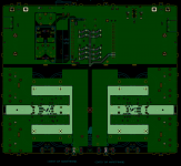
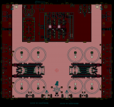
Have a look at the ground planes on one of my 4 layer boards. The main plane is on the top (red), however, on the bottom (green), I tie the bypass capacitors specifically together. The transformer center taps share the same plane on the top. It's primarily a task of eliminating loops. You cannot see the signal and signal grounding traces on either of the images, but they are run protected in an inner layer and grounds are tied together where you see the red + in the middle.
Very good results so far
S
EDIT - added signal trace image

It's always fun wondering what happened to functionality and then the 'whats this thing' that gets added. Every update is a wonder to an extent. I'm used to it now and OK anyway with it. Only two legacy features do i miss.
Have a look at the ground planes on one of my 4 layer boards. The main plane is on the top (red), however, on the bottom (green), I tie the bypass capacitors specifically together. The transformer center taps share the same plane on the top. It's primarily a task of eliminating loops. You cannot see the signal and signal grounding traces on either of the images, but they are run protected in an inner layer and grounds are tied together where you see the red + in the middle.
Very good results so far
S
EDIT - added signal trace image
Attachments
Last edited:
A zone for the ground plane doesn't have to encompass the entire ground plane. You can define regions of the plane that you want to be the same potential ground and then use a single ground trace to route it back to the power supply. You draw the zone only around the area you want to fill and connect the traces.
Without seeing your example, it is hard to know exactly what to do. But if I understand correctly, you can for example draw the ground connections in between the eight op-amps. Then you can draw a zone around the eight op-amps, and the area between the ground traces will be copper filled where possible to minimize inductance/resistance between the ground points you have connected. Then you can draw just the one trace back to the power supply. Similarly, you could draw the ground traces in the power supply, for example connecting bus capacitors to the rectifiers, regulator, etc., and the put a copper fill around that to minimize the resistance there.
If you widen the zones enough you can find that all that may really be required is a single zone with small cutouts to force the potential to be nearly constant at the points where the separated regions connect.
I guess my philosophy is that you are paying for all that copper on the board, you might as well use it.
So do I define a "zone" for each portion of my star ground? My board consists of 8 opamps, and I have routed the ground connections of each opamp circuit together, and then one connection to my power supply ground. So how do I tell KiCad to tie the ground pours (front side and back side) to only connect to the power supply ground at ONE point?
🙂
I guess my philosophy is that you are paying for all that copper on the board, you might as well use it.
Another very very nice feature in KiCAD is the ability to preview the solder paste layer using the 3D viewer. It's not much of a big deal when designing for larger parts usually, but when designing using parts with 0.5mm pitch, the paste layer can become a tricky thing. Usually, you can find it better to shrink the aperture of the paste layer to keep from applying too much solder paste onto small pads, running the risk of bridging the pins together. This way, the fab house will read the paste layer to your liking, versus just using the pad dimension as default.
In the image, you can see the gray is for the solder paste and the copper color remains free of the paste. I shrink that paste size for larger parts too in that I don't want them to float too high off the board when finished.

In the image, you can see the gray is for the solder paste and the copper color remains free of the paste. I shrink that paste size for larger parts too in that I don't want them to float too high off the board when finished.
I guess one approach would be to go to a four-layer board, with separate layers for ground and power, in addition to the normal front and back. How much more expensive is it to add two layers? My board is ~ 3" x 3".
If ordered from JLCPCB, it appears to be $2 for the two layer and $7 for the four layer.
You'll have to play around with the options some which will change the prices. I always like a different color than the basic green. Black usually doesn't cost any more but may take an extra day or two to have made.
Also, take some moments to read up on some of the articles online or elsewhere about power and ground planes. Since all of my projects so far are for personal uses, I can do things like ground lifts and the like without legal issues etc.. These things aren't big issues when you run things like ground lifts in traces, since the trace will act as a fuse, yet, when you do things like separating grounds using planes, you would be able to carry large currents in the event of a short. Be creative and wise. You are well on your way to being able to call yourself an engineer!
ALSO!
Keep in mind that the fab shop will most likely use different copper thickness in outer and inner layers!!
I try to use my high current traces and pours on the outside coppers, since these are usually the more copper thickness. Shouldn't be any such issue with opamps and small signal tho. Technically, one could also run into issues with high currents and temperatures on the inner layers first as well. Not a concern with small signals and power with opamps tho!
I place power planes on the two inner layers, and route signals and ground on the outer layers. I use net ties to isolate noisy high current paths on transformer center taps, rectifiers and filter caps. I use polygon pours for planes, and use keep outs to control where the plane goes. I use a combination of star grounding and planes.
I rarely route ground traces except for high current paths in order to keep them out of the ground plane. I stitch the upper and lower planes together with lots of vias.
I rarely route ground traces except for high current paths in order to keep them out of the ground plane. I stitch the upper and lower planes together with lots of vias.
- Home
- Design & Build
- Software Tools
- KiCAD for beginners