K-Multiplier boards for sales!
K-Multiplier boards for sales!
Hi, I am thinking about doing some fund raising for Keantoken. As some of you may know that he graduated from high school last year and he has not had any income yet. He has done many of us big favours by helping us in our DIY efforts. I personally know that he simply doesn't have money to buy parts for his project work. I have financed him some parts, his signal generator, oscillioscope and measurement soundcard, but I am financially very tight at the moment and could only wish I could do more.
I have designed a K-Multiplier PCB in ExpressPCB to be used as my Marantz SA11S1 pre-regulator. The board includes transformer secondary snubber, rectifier diodes, diode snubber, a CLRC filter and the K-Multiplier. It is designed for handling 300mA constant current with 1.4V voltage drop only. It can tolerate at least around 7,000uF (tested) at it output without damage by the inrush current. With a single 1200uF at its output, combined with the heavy duty CLRC filter, it is simulated to have ripple rejection of -61dB at 20Hz, -74dB at 100Hz (mains rectified frequency), -156dB at 10kHz, -174dB at 100kHz, and -143dB at 1MHz. So noise above 1kHz is basically non-existent. My simulation included parasitics.
I ordered the PCBs from ExpressPCB. The set up fee was $66 and the shipment fee to Sydney was $60 (that was robbery by ExpressPCB). The boards themselves did not cost that much. I need 3 for my own use and 2 for spare. Since the boards are relatively cheap after the set up fee and shipment, I ordered 10 for USD$204.
So now I have 5 to spare. I am thinking about selling each of the 5 boards at USD$45 plus shipment. All income of the board sale will go to Keantoken for him to buy parts for his project work. If I could sell all 5 then I would raise $225. It is only a small thing we can do to show we appreciate Keantoken's work. Note that you are not only buying a board for your own use but also doing some charity work. I think that is not overly expensive, and personally I paid $204 for practically 3 boards.
If you want a board please register your interest here or send me a private email. Note that I am not selling them yet until I build it and fully test it and be sure that the PCB design works as intended and it is bug free. This may happen in the coming 3-4 weeks.
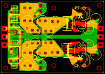
The board size is about L94mm x W66mm. It is a low profile design so that it can comfortable fit in a CD player. Capacitors are expected to be all Panasonic FR 25V 1200uF. See the attached image. The design featured a 2 layer PCB with small power and ground zones / planes to reduce inductance. Note that the current loop is made very small after the bridge rectifier.
Regards,
Bill
K-Multiplier boards for sales!
Hi, I am thinking about doing some fund raising for Keantoken. As some of you may know that he graduated from high school last year and he has not had any income yet. He has done many of us big favours by helping us in our DIY efforts. I personally know that he simply doesn't have money to buy parts for his project work. I have financed him some parts, his signal generator, oscillioscope and measurement soundcard, but I am financially very tight at the moment and could only wish I could do more.
I have designed a K-Multiplier PCB in ExpressPCB to be used as my Marantz SA11S1 pre-regulator. The board includes transformer secondary snubber, rectifier diodes, diode snubber, a CLRC filter and the K-Multiplier. It is designed for handling 300mA constant current with 1.4V voltage drop only. It can tolerate at least around 7,000uF (tested) at it output without damage by the inrush current. With a single 1200uF at its output, combined with the heavy duty CLRC filter, it is simulated to have ripple rejection of -61dB at 20Hz, -74dB at 100Hz (mains rectified frequency), -156dB at 10kHz, -174dB at 100kHz, and -143dB at 1MHz. So noise above 1kHz is basically non-existent. My simulation included parasitics.
I ordered the PCBs from ExpressPCB. The set up fee was $66 and the shipment fee to Sydney was $60 (that was robbery by ExpressPCB). The boards themselves did not cost that much. I need 3 for my own use and 2 for spare. Since the boards are relatively cheap after the set up fee and shipment, I ordered 10 for USD$204.
So now I have 5 to spare. I am thinking about selling each of the 5 boards at USD$45 plus shipment. All income of the board sale will go to Keantoken for him to buy parts for his project work. If I could sell all 5 then I would raise $225. It is only a small thing we can do to show we appreciate Keantoken's work. Note that you are not only buying a board for your own use but also doing some charity work. I think that is not overly expensive, and personally I paid $204 for practically 3 boards.
If you want a board please register your interest here or send me a private email. Note that I am not selling them yet until I build it and fully test it and be sure that the PCB design works as intended and it is bug free. This may happen in the coming 3-4 weeks.
The board size is about L94mm x W66mm. It is a low profile design so that it can comfortable fit in a CD player. Capacitors are expected to be all Panasonic FR 25V 1200uF. See the attached image. The design featured a 2 layer PCB with small power and ground zones / planes to reduce inductance. Note that the current loop is made very small after the bridge rectifier.
Regards,
Bill
Attachments
Last edited:
Oops! 1.4V drop is for the KM. The CLRC filters drops 0.2V for 300mA current. So it is 1.6V drop in total.
I like the grounding layout with the strings of stars from noisy to quiet.
I also like the overlay of power planes over grounding planes.
BUT !!!!
there is a mistake. I see the resistor passing across a gap in the ground. Where is the return route? It should be directly under the resistor. Maybe just delete the resistor and connect the ground plane between the two nearest caps.
Similarly rotate the two power transistors so that they stay very close to the grounding link.
Thanks, Andrew.
The resistor is the R=0.22R within the CLRC. It is there to provide damping so that there is no peaking in the CLC circuit. 0.22R is chosen after extensive modelling, as we want the smallest resistance without peaking so that the voltage drop is minimized.
The ground planes are surrounding the 2 Cs. The R is in between. It is mounted vertically to save space therefore its corresponding "ground area" is very small. To do it correctly, this resistor must be moved to the middle ground line. But this is not practical and can cause other problems and definitely require more space. Note that the "entrance" to the C and the "exit" from the C forms a "line", so that current can be shared between all 3 Cs. In this way, the inductor and the resistor must be positioned where they are currently positioned.
So unfortunately, somewhere somehow we must make some compromises.
I extended the ground area to cover the area of the emitter of the transistors. I have not covered the collector output copper area which would have further reduced the output inductance. If I did so, the voltage reference of the KM would have higher capacitance. So it is all about compromises.
At the end of the day, this is supposed to be a pre-regulator. It has achieved very outstanding line rejection up to some -174dB at 100kHz so a little bit noise in the impecfect PCB layout is not a big deal. There is the next stage regulator which will provide further noise reduction, and finally, there is the actually circuit that provides PSRR. The most import consideration is to keep the current loop after the rectification short, and this has been achieved very well.
The purpose of the CLRC and KM is to reduce higher frequency ripples to basically nothing. This makes the next stage regulation much easier and much more stable with far less chance of oscillation.
I understand compromises.
I also understand Ott's "rule":
Never have a component current or trace current passing over/across a split in a plane. That split forces the return current to find an alternative route that MUST have a HIGHER impedance.
I also understand Ott's "rule":
Never have a component current or trace current passing over/across a split in a plane. That split forces the return current to find an alternative route that MUST have a HIGHER impedance.
You may want to consider adding a wideband ferrite choke for additional HF / VHF filtering. They're rated for 5 amps so your 300mA design won't tax their capabilities, and the price is low: 27 cents per piece @ qty=100. (sales link) Since they're inherently lossy at HF (but not DC) they don't require additional components for damping. And the board footprint is small.
I just bought 100 of the Bourns FB2002-4B-RC for this purpose, and design work is underway.
I just bought 100 of the Bourns FB2002-4B-RC for this purpose, and design work is underway.
Attachments
Hi Bill
Quote: It is designed for handling 300mA constant current with 1.4V voltage drop only
Can we use this board to feed a ccs running at 600mA "each side" ?
Quote: It is designed for handling 300mA constant current with 1.4V voltage drop only
Can we use this board to feed a ccs running at 600mA "each side" ?
I understand compromises.
I also understand Ott's "rule":
Never have a component current or trace current passing over/across a split in a plane. That split forces the return current to find an alternative route that MUST have a HIGHER impedance.
You are right. But in this particular case that higher impedance route is the extra 17mm track of more than 5mm width. Putting it into a calculator shows Z=0.00022R + j 0.048025R at 10MHz and Z=0.00279R + j 3.44235R at 100MHz. The wires between boards will completely swamp this.
You may want to consider adding a wideband ferrite choke for additional HF / VHF filtering. They're rated for 5 amps so your 300mA design won't tax their capabilities, and the price is low: 27 cents per piece @ qty=100. (sales link) Since they're inherently lossy at HF (but not DC) they don't require additional components for damping. And the board footprint is small.
I just bought 100 of the Bourns FB2002-4B-RC for this purpose, and design work is underway.
Good suggestion. This may be a product I may use next time.
I rarely thought of noise at such a high frequency because a 20cm wire would have 143R at 100MHz. It is necessary for small device such as mobile phones. But then these days I can never know as I can't rely on my cheap 100MHz digital oscillioscope to tell me anything at this frequency, and all the wireless networks may create a lot of noise. Fortunately I don't live near a transimitter.
That 47uH inductor on the PCB is for the one made by Wurth (7447471470). It has a fres=9MHz and is shielded. 9MHz is pretty good for 47uH.
Hi Bill
Quote: It is designed for handling 300mA constant current with 1.4V voltage drop only
Can we use this board to feed a ccs running at 600mA "each side" ?
Keantoken suggested that the standard KM performs best below 500mA. The pass transistors may run above 1A current but perhaps performance won't be as good above 500mA. I have just simulated for 600mA and it did not show anything bad at all. You had better check with Keantoken though. For 300mA current, you don't really need a heatsink but it will run hot, so I put a small heatsink there. If you want to run 600mA, you would need to increase the heatsink size. The dissipation is 1.6V * 0.6A = 0.96W. You need a heatsink with 20 degree per W rating. You should still be able to find one that fits into that PCB. You may also need to increase the CLRC capacitance because ripples are higher for 600mA. This is not a big deal because you can select capacitors with the same diametre but taller.
Note that the standard KM is designed for low voltage use, not high voltage. So it won't work with Salas HVSS shunt.
Hi Bill
Quote: It is designed for handling 300mA constant current with 1.4V voltage drop only
Can we use this board to feed a ccs running at 600mA "each side" ?
Do you mean +/-V rails? or two +V rails?
The board is designed for +/-V rails with input from a two secondary windings of a transformer. However, I have just looked at the PCB, it may be possible to use it for two +V rails, if you use the right parts, swap the polarity of components. But you may need to fiddle with the input though.
How does the radiated field of a bead compare to that of a coil of the same inductance? A bead is like a tiny toroid so I suspect it will have less coupling with local fields.
@keantoken
I have a problem when I take off the caps between the valve rectifier & your CFP cap multiplier: the voltage droped to 150V🙁
I have a problem when I take off the caps between the valve rectifier & your CFP cap multiplier: the voltage droped to 150V🙁
Do you mean +/-V rails? or two +V rails?
The board is designed for +/-V rails with input from a two secondary windings of a transformer. However, I have just looked at the PCB, it may be possible to use it for two +V rails, if you use the right parts, swap the polarity of components. But you may need to fiddle with the input though.
I am planning to use both +v rails at 600mA
@keantoken
I have a problem when I take off the caps between the valve rectifier & your CFP cap multiplier: the voltage droped to 150V🙁
The caps have to be there or the voltage transient and/or inrush destroys the Kmultiplier. I guess I should have made that clear. Incidentally, it will help me to know which transistors are blown, if not both of them.
Do not change R5 and C4 and do not increase C1 over 82uF. Use no more than 330uF at the output.
My psu have 220uF 75R 220uF so I have R5 75R, it's OK?
It's necessary a cap between the multiplier & the SSHV2?
Please send me a PM with your paypal account to donate something to help you.
It's necessary a cap between the multiplier & the SSHV2?
Please send me a PM with your paypal account to donate something to help you.
- Home
- Amplifiers
- Power Supplies
- Keantoken's CFP cap multiplier