DC servos and JFET pairs
Here are a couple of more thoughts on DC servos.
While some prefer JFET input pairs for reasons of sound quality and EMI resistance, there is another reason that makes them attractive. The fact that JFET input stages do not suffer from input bias current offset makes the job of the dc servo much easier.
If an amplifier is to have a reasonably high input impedance, its input base or gate return resistor must be large, at least 20k. BJT input bias current flowing through this resistor will cause a far larger offset than the input voltage offset of the input pair, or of input-referred offset from the VAS stage.
Bear in mind that a BJT input stage often wants to be biased in the milliampere range for low noise, high speed, low distortion, and immunity to EMI. This necessarily results in high input bias currents on the order of 1-10 uA. An input BJT biased at 1 mA with a beta of 200 will have a base current of 5 uA. This current flowing through a 20k input return resistor will cause a voltage drop of about 100 mV. In conventional designs using an electrolytic capacitor in the feedback return leg, a feedback resistor from the output with the same value of 20k will see the same drop. The offset consequences of the BJT input bias current will then largely be canceled out to the extent that the betas of the input pair are reasonably matched.
When we ditch the electrolytic capacitor and employ a dc servo instead, we are not so fortunate. With the servo arrangement (sans the electrolytic capacitor), the dc return resistance on the feedback side of the input stage is very low, perhaps on the order of 1k or less. In the absence of servo action, the amplifier now suffers from a substantial 100 mV input-referred dc offset due to the drop across the input return resistor. This offset is much worse than the 5-20 mV input offset we may see with JFETs. BTW, if high-beta input transistors are used, they may not have a very high voltage rating, and may need to be cascoded (just like one often has to do with a JFET input stage).
If a JFET input stage is used instead, there is no input-bias-current-induced offset, and the servo need only compensate for the 5-15 mV of offset of the JFET pair.
The bottom line here is that the servo must typically work much harder when used in a typical dc servo arrangement with BJT input pairs as opposed to JFET input pairs. And it will be operating at a one-sided value of servo output offset, which, if not compensated in some way, will diminish its value as an indicator of proper operating status.
Thoughts? Did I get this right?
Cheers,
Bob
I actually prefer a real offset on the servo. Then, it is working only on one side and not going through the xover region as often, if at all.
PMA said:Yes, only SO-8. I use reductions if I need them in a non-SMD PCB. Nice part, High OLG, high Ft, high SR, fast, very stable, not so much FB.
What do you mean in this context by "not so much FB"? And how's an opamp with "to much FB"?
john curl said:I actually prefer a real offset on the servo. Then, it is working only on one side and not going through the xover region as often, if at all.
Hi John,
Yes, this is a good point. However it is easily achieved by the old technique of hanging a load resistor to the negative rail.
Cheers,
Bob
Usually, you have to trade off gain for open loop bandwidth at low frequencies. We prefer LESS global feedback and a higher open loop bandwidth. This also forces better open loop linearity, since it cannot be covered up by feedback. Most of my designs use moderate feedback, but I find that less feedback is better, an more attention should be addressed to making each stage as linear as possible.
john curl said:Usually, you have to trade off gain for open loop bandwidth at low frequencies. We prefer LESS global feedback and a higher open loop bandwidth. This also forces better open loop linearity, since it cannot be covered up by feedback. Most of my designs use moderate feedback, but I find that less feedback is better, an more attention should be addressed to making each stage as linear as possible.
John,
First, making each stage as linear as possible and feedback are not necessary mutually exclusive. Your design philosophy was beated to death here and (although I disagree with you) I am not the one attempting to try to change your mind. However...
Should I understand "not so much FB" as "not so much FB required"? If so, I am even more confused. If the opamp has high gain-bandwidth product, and if the closed loop gain is a design requirement, then such a "good" opamp will have more closed loop BW and more loop gain at HF to reduce distortions, etc... - something that I understand you are not advocating.
What I am trying to say is that for opamps "not so much FB required" doesn't make much sense. While in a discrete design one can trade the open loop gain for linearity (usually by using local feedback like emitter degeneration, etc...) and then using low global FB, such an approach is usually not possible in an opamp gain stage. That's why I would describe "not so much FB" in the context of opamps as just another tongue-in-cheek sintagm intended to impress the n00bs around.
BTW, AD825 is indeed a very good opamp, in particular when it comes to the cost/performance ratio. Otherwise, in a "no cost objection" environment, there are better solutions even from AD (and I'm thinking at least of AD797 and AD745 and my late favourite ADA4899-1 (not JFET input, though)).
I thought giving folks at BA something that nobody can buy would be fun.
Variac - Maybe next year we could pre-arrange a better way for me to give away samples of things people might use in their DIY projects.
Variac - Maybe next year we could pre-arrange a better way for me to give away samples of things people might use in their DIY projects.
scott wurcer said:...a better way for me to give away samples of things people might use in their DIY projects.
I'll PM my mailing address.
🙂
...or for breadboarding of a future SMD production.
Thanks again Scott!
I was waiting for BB samples from TI, but probably I may go with AD parts.
Thanks again Scott!
I was waiting for BB samples from TI, but probably I may go with AD parts.
It is almost impossible to have a perfectly linear input stage and high open loop bandwidth. This is because the first stage gain is all important for high gain, and low noise demands that you avoid local feedback through emitter or source degeneration.
Yup Scott , the show is a work in progress. The reason we auctioned some stuff off was not because we were desparate for money but because I felt that people would only bid on stuff that they really wanted.(they generally didn't bid much anyway) That is also why I gave the grand prize lottery winner a choice between the ribbon tweeters or 2 Passie Chassis. We probably should have auctioned your chips too. Still, I got some and I thank you.
Mark
Mark
I'm glad also that you just gave them away. I would not have bid on them, and I would have lost the chance to try, especially, the 815. I did have an 825 here, that Walt Jung sent me, but I did not have any quantity to try them in a design.
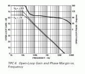
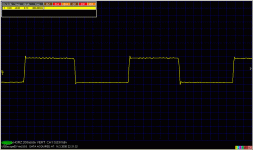
PMA said:And, it has almost perfect time response. Measured with probe 1 :10, so amplitude is 10x higher than reading.
Sound of AD825 is :bs: IMHO
john curl said:Why would it sound bad? Any opinions on the matter?
I have no idea, tried it as IV-converter after DAC some years ago when the part was just released.
re Bob's post9961:
the AC coupled amp with matching resistances on the two inputs has an inherently matched offset that cancels. No DC servo is required if the required semis are matched and kept in temperature range.
Remove the DC blocking cap from the NFB leg and the amp becomes a mixed AC & DC coupled monstrosity that inherently has an unmatched output offset. I repeatedly recommend this should never be done, not even when using a DC servo to cover up the topology error.
Remove the DC blocking cap at the input as well as at the NFB leg and create a DC coupled amp. Now the source resistance can be made to match the NFB resistance and we are back to the self canceling set up.
This inherently stable system is ideally suited to a DC servo, but must also have DC detect and isolation in case the source and/or amplifier becomes faulty.
A "nice to have" would be DC detect and input muting that removes the possibility of source induced offset, this also covers for interconnects that are removed or intermittent.
Using this arrangement, the DC servo would adjust for operating temperature changes in offset, the basic amplifier would be set up from a cold start with minimum output offset with the actual source resistance in place.
I contend that amps should be AC coupled
or
DC coupled with DC servo and DC detect with output isolation.
- Status
- Not open for further replies.
- Home
- Amplifiers
- Solid State
- John Curl's Blowtorch preamplifier