Plating the barrels of the holes would be interesting...
Quite honestly though is there any point with the range of modern materials available today....
Better to use a high speed FR4 weave such as 7268 or even a high performance laminate...
https://www.altera.com/content/dam/altera-www/global/en_US/pdfs/literature/an/an528.pdf
why go to extremes with something that is totally impossible to manufacture a board reliably
I have seen hybrids that have been made from glass already 20 years ago,
and they were not new then. With printed resistors, caps and sot-23 transistors.
I think they were from tv tuners. Contacts were like IC pins along one side,
much like SIL resistor networks. Vias were silver-filled epoxy or sth. like that.
The glass does not bend, so vias are harmless.
regards, Gerhard
It's not actually the price that bothers me... It's that I can see a ton of cheap *** parts for that price in it... and some ******* that can't even properly twist wires put it together.
Looks like it would make a really good doorstop, given it's weight...
I have seen hybrids that have been made from glass already 20 years ago,
and they were not new then. With printed resistors, caps and sot-23 transistors.
I think they were from tv tuners. Contacts were like IC pins along one side,
much like SIL resistor networks. Vias were silver-filled epoxy or sth. like that.
The glass does not bend, so vias are harmless.
regards, Gerhard
I would be interested in seeing them, drilling and filling the vias must cost the earth, as well as the conductivity through the vias...
Did find this and one or two other docs...
http://www.izm.fraunhofer.de/conten...kaging/EOCB/IEEE ECTC 2012 Schröder et al.pdf
Not exactly a glass PCB... but looks interesting.
But to be honest I can think of many factures such as its stiffness that could be detrimental, making a multilayer one would be quite interesting but again fragile.... And why, and then we get onto Dk, glass varies depending on the type from 2.8 to over 14....
There is some stuff on making a single sided PCB on a glass slide, but as said I cant see any benefit and plenty of problems.
The point is that it can be a flexible prototyping method....'rip up and retry'.Plating the barrels of the holes would be interesting...
Quite honestly though is there any point.....
The self adhesive foils can be easily trimmed/shaped with a scalpel, and slots/stars/return paths etc in ground planes can be easily implemented.
The substrate is thin enough that 'vias' can be created by virtue of access to the undersides of the foils through holes drilled (with a diamond burr ?), giving direct solder access for traces and SMD/TH components.
Remember I said this is for some audio test jigs, but just for fun this could easily be applied to preamp/line amp etc stages...this thin easily available glass substrate ($2 shops) and foil method might sound good, and it might not.
These guys have already taken this to the next level....http://www.schott.com/si102_01_thin_glass
Dan.
Self adhesive copper foil is easily available as snail/slug barrier from garden/hardware stores and shielding foil from guitar/music stores.
Last edited:
Yes, I have seen those, and of course STK modules have done this since forever on ceramic substrate.I have seen hybrids that have been made from glass already 20 years ago,
and they were not new then. With printed resistors, caps and sot-23 transistors.
I think they were from tv tuners. Contacts were like IC pins along one side,
much like SIL resistor networks. Vias were silver-filled epoxy or sth. like that.
The glass does not bend, so vias are harmless.
regards, Gerhard
Dan.
But then most of us don't have to worry about the silly temps you play with...
All my current work with glass laminates at 4.5K is structural, not electrical. I mentioned the anisotropy as being both mechanical and electrical (permittivity).
I do get called on occasionally for on board differential high speed data run concerns from time to time, but they are all near room temp application...actually, temp controlled to +/- 0.1 C. Most of my "on call" ends up dealing with EMC issues on boards, sometimes analysis of part failures.
John
Surprised its "glasses" versus, say, fused silica or the like. Of course, what has a Tg that low?!
And, yeah, this whole pcb thing seems a *wee* bit overblown (material, not layout). We're not making antennas (intentionally, at least), etc. Pick something decent and roll with it.
I would be interested in seeing them, drilling and filling the vias must cost the earth, as well as the conductivity through the vias.
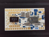
Not glass but ceramic: the TDS series Tektronix oscilloscopes attenuators and input stage circuitry. Double sided, thin film deposited resistor (laser adjusted) vias, gold traces, one IC, shortly a piece of jewelry.
Attachments
Sorry, I meant glass cloth laminates.Surprised its "glasses" versus, say, fused silica or the like. Of course, what has a Tg that low?!
And, yeah, this whole pcb thing seems a *wee* bit overblown (material, not layout). We're not making antennas (intentionally, at least), etc. Pick something decent and roll with it.
As to DA, my hi-pot training course stresses VERY heavily that aspect. If I bring a magnet to 5kV for 60 seconds, then short it for 5 seconds only, it climbs up very fast to kv levels again due to DA. We require short for as long as the voltage was applied. Honestly, I tell them to keep it shorted until it is needed, no sense being foolish.
From what I recall, pease did this years ago, with what, a 4 or five stage cap/resistor model.. I don't think PCB today has the issue tek found years ago.
John
Not glass but ceramic: the TDS series Tektronix oscilloscopes attenuators and input stage circuitry. Double sided, thin film deposited resistor (laser adjusted) vias, gold traces, one IC, shortly a piece of jewelry.
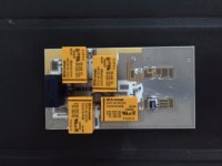
Standard hybrid stuff. I was involved in that back in '83. I assume that's alumina.
Most of the stuff I worked with was that ceramic substrate soldered or epoxied into a hermetic case with wirebonds to the package pins. Did some SIP units as well, but not much.
John
I remember being puzzled when I saw high voltage oil capacitors in labs with a very obvious shorting wire across the standoff terminals. Was it to be used for a handle I wondered 🙂Honestly, I tell them to keep it shorted until it is needed, no sense being foolish.
From what I recall, pease did this years ago, with what, a 4 or five stage cap/resistor model.. I don't think PCB today has the issue tek found years ago.
John
It's a little bit like the way you learn to treat raw aluminum pieces in an extrusion factory. Since the emissivity is so low, you might pick up a piece that is quite hot and get severe burns.
It would appear that TEK kept its own consul when it came to what substrate material to use for critical locations. Good for them, and I advise anyone to look closely at the FR-4 material that you choose. I think we can be assured that some FR-4 is far worse (even in measurement) than other FR-4 material, so I would recommend being careful. For example, FR-408 , might be a really good choice. I am certainly going to try it.
Isn't the FR4 rating just related to it flame rating and not the dialectic properties of the specific board material?
It would appear that TEK kept its own consul when it came to what substrate material to use for critical locations.
Forgot to mention, that's for a 500MHz digital oscilloscope, ~1990.
RO4350, microstrip and MMICs could do it much better and cheaper today.
It seems to me that with ground fills used on most audio pcb, there might be enough pcb cap dielectric between traces and grnd to be in the range of transistor C's. How linear is pcb C?
THx-RNMarsh
THx-RNMarsh
Last edited:
Standard hybrid stuff. I was involved in that back in '83. I assume that's alumina.
John
Not audio but the most impressive hybrid I have used is the ford EDIS module. I was a thick film hybrid potted in some sort of jelly protective goop. You could rework through the goop. Never found a reference for what it was.
Impressive because an auto OEM bothered to do that and it was so over engineered that they are almost indestructible. The off road crowd love them for engines that run underwater. And easy to drive from a simple micro. I can only assume that as this was Fords first foray into distributorless ignition they dared not mess it up.
It seems to me that with ground fills used on most audio pcb, there might be enough pcb cap dielectric between traces and grnd to be in the range of transistor C's. How linear is pcb C?
THx-RNMarsh
Good enough to use for compensation if you have a good board house that uses name brand materials.
I worked closely with Bosch and a bunch of other tier one vendors for 5 years supplying power mosfets for ECU's and ABS breaking. Auto electronics is hugely demanding and the manufacturing quality is superb - non of the suppliers take short cuts.
Alumina substrate is commonly used for hybrid modules. .
Alumina substrate is commonly used for hybrid modules. .
Last edited:
The "hook" issue Tek found was relevant for high impedance passive attenuators. Scope input was/is 5-20 pF in parallel with 1 MegOhm. A multistep attenuator could end up with some significant PCB interactions between traces with that much going on.
Back then Tek had their own PCB fab (a very nice operation) and took in outside work. I got them to make some boards for early Spectral products using the special PCB material they found for this. I forget what it was but it had no reinforcing and was clear. It was also fragile and sensitive to cleaning chemicals. Soon after ,Tek shut down the whole thing and no more "magic" PCB's. I'm not sure they made much difference but they were nice. All gold plated like HP. Really nice audio jewelry.
Back then Tek had their own PCB fab (a very nice operation) and took in outside work. I got them to make some boards for early Spectral products using the special PCB material they found for this. I forget what it was but it had no reinforcing and was clear. It was also fragile and sensitive to cleaning chemicals. Soon after ,Tek shut down the whole thing and no more "magic" PCB's. I'm not sure they made much difference but they were nice. All gold plated like HP. Really nice audio jewelry.
- Status
- Not open for further replies.
- Home
- Member Areas
- The Lounge
- John Curl's Blowtorch preamplifier part II