Sir Juma, kindly HELP; advance apologies from a non-techie about probable "stupid questions"...
I was doing the layout (post #13) on a dot-matrix board, and got stuck with how to realize the ground.
As I understand, there are two floating supplies of 20V each, derived from two separate transformer windings, bridge rectifiers and filter caps. One supply +ve feeds Q5 Drain, while its -ve (0V) is cross-connected to Q6 Source. Likewise the second 20V supply +ve feeds the Drain of Q6, while its -ve (0V) is cross-connected to Q5 Source. Both + and - are fully floating.
My problem is understanding where the ground is coming from?
We have R5/R7 junction, as also the input side of C2 connected to ground.
Is this ground a "derived one" from the series connection of R5 and R7?
While using a differential input, as you had suggested, we will have R26 and one more 100k, with their common point as signal ground.
Also, we have the series chain R3, R16, R24 and R15 across the supply, again providing a zero reference at its middle.
Kindly forgive the inability of somebody conditioned to simple power supplies and their ground/zero reference points to comprehend this arrangement. An explanation/guidance is what I need now to progress further.
Sincerely yours
Hi Prof,My problem is understanding where the ground is coming from?
Juma may have other ideas, but in my case, circuit ground is connected directly to signal ground, i.e., the ground terminal of the signal input connector. For safety, there is also a connection between signal ground and chassis (or protective earth) made through an inrush current limiter (e.g., Amphenol CL-60) or other means to help break ground loops.
Thank you, JB.
My need was for an amp to drive the speaker with a differential output, so that the chain from DAC thru pre to power would all be differential/balanced, and Juma kindly pointed me to this thread. Yes, I follow the recommended practice of making Pin1 of the XLR connector chassis ground, and that works flawlessly.
My difficulty here was trying to understand how the circuit ground was derived, with the two separate supplies floating.
Perhaps if a circuit with DC voltages at the major nodes was posted, it would help us non-techies to understand the working of the circuit better.
The best would be a "teach-in" by one of the masters!
🙂
Thanks and warm regards.
It may help to imagine the amplifier as a portable device in which the two separate supplies are batteries. If we apply an input signal from another battery-powered portable device, the amplifier still works fine but "ground" no longer represents any kind of connection to earth. Instead, ground serves only as a reference point for passing a signal from one component to another.My difficulty here was trying to understand how the circuit ground was derived, with the two separate supplies floating.
The situation here is the same as in the portable example, except that "ground" is now referenced to earth for signal compatibility with other earth-referenced components. In terms of basic amplifier operation, ground has no other function, and is not so much derived as simply assigned.

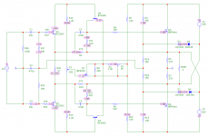
As a possible aid to understanding, here is a snapshot from an MC12 sim of Juma's post #13 version of the circuit showing all DC node voltages with the amp at temperature and no signal applied. Of course, this is a simulation so don't expect to see this level of precision and balance in real life. (OTOH, with matched components I've come surprisingly close...)
One thing to note here is that the Vds across Q7 at about 1.4V is rather low, which might account for the problem Minek saw in his post #45 model. This likely wouldn't be a problem when driving the input balanced, as there is very little signal modulation across Q7 in that case. When driven unbalanced, there may be enough signal across Q7 to shut it off intermittently. A possible solution is to reduce the R13-R14 values to allow 2V or more Vds across Q7 at idle.
One thing to note here is that the Vds across Q7 at about 1.4V is rather low, which might account for the problem Minek saw in his post #45 model. This likely wouldn't be a problem when driving the input balanced, as there is very little signal modulation across Q7 in that case. When driven unbalanced, there may be enough signal across Q7 to shut it off intermittently. A possible solution is to reduce the R13-R14 values to allow 2V or more Vds across Q7 at idle.
Attachments
Sorry I am a bit late responding ... was out of station.
Thank you JB for that explanation and the voltage readings. It has been a good learning experience...let me go over the circuit again a couple of times.
🙂
I shall keep that Q7 snafu and the R13-14 values in mind for when building. Hope by that time Juma chimes in with an easy solution. (My supplier has refunded the money, as he has no stocks now of the MOSFETs ... trying another one...)
I have one doubt-- the differential audio signals appear across the speaker. So the DC output offset is to be measured (and corrected with P1) from the ground reference and any one speaker terminal?
You would measure DC output offset as seen by the loudspeaker, so between the speaker terminals. P1 only affects this offset. There is no adjustment as such in this circuit for absolute DC offset, measured from each speaker terminal to ground. That's usually OK, because absolute DC offset is irrelevant to a floating load such as a passive speaker.So the DC output offset is to be measured (and corrected with P1) from the ground reference and any one speaker terminal?
As a matter of (mostly academic) interest, any residual absolute DC offset in this design would be due to DC leakage currents through R5 and R7. Although unwanted, some small leakage current is to be expected in real circuits due to imperfect insulation and dielectric materials. For example, I recall measuring about 30 mV of absolute DC offset in one of my early designs that also used 270 ohms for R5 and R7, implying about 110 uA leakage through each resistor.
It’s possible that the Vas stage in Juma’ circuit clipped before Q7 ran out of headroom, in which case it wouldn’t have been apparent. We see it in the sim partly because the power supplies don’t sag under load, delaying Vas clipping vs. the real circuit.I shall keep that Q7 snafu and the R13-14 values in mind for when building. Hope by that time Juma chimes in with an easy solution.
Could you please help in understanding regarding Q7 mosfet in this topology.
Here its source is connected to power supply and gate is connected to output of Q3, Q4. And drain of Q7 is connected to output of Q1, Q2.
Also again it seems like Q7 is providing the power supply to the loops of Q1, Q2 and loop of Q3, Q4. It is confusing what Q7 is doing here, and how it is enabling it to use output MOSFETs without emitter degeneration resistors.
Also can we use BJT BC546BTA and BC556BTF instead of BC550, BC560 (these seems to be discontinued) or which other alternatives we may use for these BJTs?
And cost of these BJTs are very very less compared with JFETs, so do they perform well compared with JFETs?
And cost of these BJTs are very very less compared with JFETs, so do they perform well compared with JFETs?
A small tutorial would sure be of help to many of us ...Could you please help in understanding regarding Q7 ....
The use of Q7 here is indeed a uniquely clever application.
Thanks in advance.
Last edited:
Before discussing Q7 in particular, let me briefly review the overall design of the circuit just to be sure that we have a common understanding.Could you please help in understanding regarding Q7 mosfet in this topology.
For this purpose I've redrawn the circuit here in simplified form, using JFET input devices and a symmetrical layout that mostly avoids potentially confusing wire crossings. Component labeling is also simplified, so it does not always correspond to the labeling in the more complete schematics presented earlier.
The forward signal path now flows from the center of the drawing outward, as follows:
Input stage Q1-Q2 receives the INPUT signal, compares it to the signal appearing across R5, and presents a difference signal to the Vas stage across R6-R7. The signal across R5 is derived from the R3-R5-R4 string and defines the closed-loop gain of the amplifier. Resistors R1-R2 reference the INPUT terminals to ground and R12-R13 do the same for the SPKR terminals.
The input stage draws operating current from power supplies V1-V2 at the junction of resistors R10-R11, at which point the opposing signal swings on the power supplies largely cancel out, leaving a more-or-less constant DC voltage. Q1-Q2 return their operating currents to V1-V2 separately through R3-R4, bypassing ground. Resistors R3-R4 also set DC bias for Q1-Q2.
Voltage gain (Vas) stage Q3-Q4 is a differential pair biased by constant current source CCS, which also acts as the bias current source for the output stage. This stage amplifies the signal across R6-R7 and delivers differential drive currents to R8-R9 to drive the output stage. Like the input stage, the Vas stage also draws operating current from the junction of R10-R11 and returns it to V1-V2 separately through R8-R9, again bypassing ground.
Output stage Q5-Q6 is configured as a circlotron, as indicated by the cross-coupling seen at the top of the drawing. Under no-signal conditions, the DC bias currents through vertical MOSFETs Q5-Q6 are ideally balanced, and no net current flows in the SPKR load. When signal is present across R8-R9, the stage becomes unbalanced, sending current through the SPKR in one direction or another, once again bypassing ground.
This output stage operates in transconductance mode, meaning that it converts the drive voltages appearing across R8-R9 into currents without regard to the actual voltages appearing at the SPKR terminals. Global negative feedback is therefore applied to the input stage via R3-R5-R4 to control the output voltage by comparing it to the input and amplifying the difference.
Now let's return to bias current source CCS. For the circuit to work well in practice, CCS must 1) enforce differential action in Q3-Q4 so that Q5-Q6 are driven in a balanced manner; 2) be adjustable to allow for precise setting of the output stage bias; and 3) automatically adjust its output current over time to compensate for the tendency of the Q5-Q6 bias current to increase as temperature rises.
There are a variety of known ways to implement a CCS to do this. The solution used here was chosen for its relative simplicity and its ability to effectively and dynamically correct imbalances in Vas stage operation. The next figure is identical to the first, except that CCS is replaced by this solution in its simplest form.
Here, resistor R14 forms the main current path from the R10-R11 junction through Q3-Q4, and hence also through R8-R9. It is easily adjustable, of course, but does not perform well as a current source and does not provide temperature compensation.
To provide these enhancements, we add a control loop around Q3-Q4 with P-channel MOSFET Q7 acting as a control element. Q7 compares the voltage across R14 with its own Vgs and conducts the current needed to shift R6-R7 up or down so as to dynamically stabilize this voltage.
Given that Q7 is placed in the same thermal environment as Q5-Q6 and has the same Vgs temperature coefficient, Q7 will adjust the voltage across R14 downward to match its own declining Vgs over temperature, which in turn will adjust the current through R8-R9 downward and with it the Vgs seen by Q5-Q6, stabilizing the output stage bias current.
I hope this answers most of your questions. For others I didn't anticipate, please let me know and I'll try to clarify further.
Last edited:
Juma reports that high-beta BJTs sound best, but they do not self-bias like JFETs, so you will need to add a DC bias and AC coupling to the inputs as shown in post #13. The input operates at line level, so the higher noise spec of BC546/556 et al should not be an issue here.Also can we use BJT BC546BTA and BC556BTF instead of BC550, BC560 (these seems to be discontinued) or which other alternatives we may use for these BJTs?
And cost of these BJTs are very very less compared with JFETs, so do they perform well compared with JFETs?
Last edited:
Hi Joe,Before discussing Q7 in particular, let me briefly review the overall design of the circuit just to be sure that we have a common understanding.
For this purpose I've redrawn the circuit here in simplified form, using JFET input devices and a symmetrical layout that mostly avoids potentially confusing wire crossings. Component labeling is also simplified, so it does not always correspond to the labeling in the more complete schematics presented earlier.
The forward signal path now flows from the center of the drawing outward, as follows:
Input stage Q1-Q2 receives the INPUT signal, compares it to the signal appearing across R5, and presents a difference signal to the Vas stage across R6-R7. The signal across R5 is derived from the R3-R5-R4 string and defines the closed-loop gain of the amplifier. Resistors R1-R2 reference the INPUT terminals to ground and R12-R13 do the same for the SPKR terminals.
The input stage draws operating current from power supplies V1-V2 at the junction of resistors R10-R11, at which point the opposing signal swings on the power supplies largely cancel out, leaving a more-or-less constant DC voltage. Q1-Q2 return their operating currents to V1-V2 separately through R3-R4, bypassing ground. Resistors R3-R4 also set DC bias for Q1-Q2.
Voltage gain (Vas) stage Q3-Q4 is a differential pair biased by constant current source CCS, which also acts as the bias current source for the output stage. This stage amplifies the signal across R6-R7 and delivers differential drive currents to R8-R9 to drive the output stage. Like the input stage, the Vas stage also draws operating current from the junction of R10-R11 and returns it to V1-V2 separately through R8-R9, again bypassing ground.
Output stage Q5-Q6 is configured as a circlotron, as indicated by the cross-coupling seen at the top of the drawing. Under no-signal conditions, the DC bias currents through vertical MOSFETs Q5-Q6 are ideally balanced, and no net current flows in the SPKR load. When signal is present across R8-R9, the stage becomes unbalanced, sending current through the SPKR in one direction or another, once again bypassing ground.
This output stage operates in transconductance mode, meaning that it converts the drive voltages appearing across R8-R9 into currents without regard to the actual voltages appearing at the SPKR terminals. Global negative feedback is therefore applied to the input stage via R3-R5-R4 to control the output voltage by comparing it to the input and amplifying the difference.
View attachment 1070792
Now let's return to bias current source CCS. For the circuit to work well in practice, CCS must 1) enforce differential action in Q3-Q4 so that Q5-Q6 are driven in a balanced manner; 2) be adjustable to allow for precise setting of the output stage bias; and 3) automatically adjust its output current over time to compensate for the tendency of the Q5-Q6 bias current to increase as temperature rises.
There are a variety of known ways to implement a CCS to do this. The solution used here was chosen for its relative simplicity and its ability to effectively and dynamically correct imbalances in Vas stage operation. The next figure is identical to the first, except that CCS is replaced by this solution in its simplest form.
View attachment 1070793
Here, resistor R14 forms the main current path from the R10-R11 junction through Q3-Q4, and hence also through R8-R9. It is easily adjustable, of course, but does not perform well as a current source and does not provide temperature compensation.
To provide these enhancements, we add a control loop around Q3-Q4 with P-channel MOSFET Q7 acting as a control element. Q7 compares the voltage across R14 with its own Vgs and conducts the current needed to shift R6-R7 up or down so as to dynamically stabilize this voltage.
Given that Q7 is placed in the same thermal environment as Q5-Q6 and has the same Vgs temperature coefficient, Q7 will adjust the voltage across R14 downward to match its own declining Vgs over temperature, which in turn will adjust the current through R8-R9 downward and with it the Vgs seen by Q5-Q6, stabilizing the output stage bias current.
I hope this answers most of your questions. For others I didn't anticipate, please let me know and I'll try to clarify further.
Very very thanks for the detailed description of the circuit 👍👍👍. With this redrawn circuit now its more clear how the circuit is functioning.
May be we can include a link to this post in the first post of the thread for reference for others.
Ah, a master class by 'Prof' JB !!Before discussing Q7 in particular, let me briefly review the overall design of the circuit ...
Thank you indeed.

That would be the thermal bias compensation provided by Q7, as described near the end of post #72. No further means of stabilizing the output stage bias (such as adding source resistors) are needed.
It may help to imagine the amplifier as a portable device in which the two separate supplies are batteries. If we apply an input signal from another battery-powered portable device, the amplifier still works fine but "ground" no longer represents any kind of connection to earth. Instead, ground serves only as a reference point for passing a signal from one component to another.
The situation here is the same as in the portable example, except that "ground" is now referenced to earth for signal compatibility with other earth-referenced components. In terms of basic amplifier operation, ground has no other function, and is not so much derived as simply assigned.
I answered my own question on this when building my tube hybrid circlotron. I simply have a star ground and everything references from that.
Thanks NickKUK, you raise a good point: you don't always need to isolate signal ground from chassis ground. I've had ground loop noise issues in my systems in the past, so I just do it as a matter of habit. Cheap insurance, but you don't always need it.I simply have a star ground and everything references from that.
- Home
- Amplifiers
- Solid State
- Joe Berry's Circlotron