I didn’t even think about the low side, only seeing one gate get a wave on the 4 output FETs (2 high / 2 low) should have been an indicator, didn’t even realize each side has its own chip, is that common? Are there always separate chips for both high and low side? Just thinking about it now the Alpine M650 I’m repairing has 2x IR2010S chips, assuming on for each side?
I am not getting a wave on the low end, which is 4.3v @ each FET gate, both high side FET gates now have a 5.3v square wave.
I’m going to see if I can find another 4427, or what would be a low side driver ic to the 4427 if it’s a high side only IC, I’m still learning how each chip can be used, etc. you can easily see why engineering/etc needs so many years to get a degree in ...and this is just one aspect/field of it lol. Just wow ...I never did like the easy way to anything tho so 🤓 lol.
Is the 4.3v pure DC?
What do you have on the output of the 4427?
The 4427 drives the low-side.
Why do you want another 4427?
If you went for a degree in electronic design, they probably wouldn't cover much in the way of circuits like this. It's more the components that make up the circuits and how they work.
Some circuits use driver ICs like the IR20xx and the IRS21844 but many designs are discrete or a mix of discrete and ICs of various types.

Looks to be -4.3v dc, no frequency although scope says 1-1.2vPkPk?
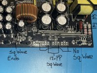
4427 out pin 7 @ 12vPkPk w/square wave
4427 out pin 2 @ 6vPkPk square wave
both FET gates with waves @ 12PkPk squarewaves
Just my newbness assuming is all, sometimes I forget just how many different ways there are to do the same thing with amplifiers, I know some tech still being used is 10/20+ years old and then there’s new unique 1 off designs, need to take each amp as its own and try not to compare to other boards I’ve worked on in the past.
So I can see the wave stops at each of the 1281 resistors on both sides, but they both read within spec 1.82k Ω, would I be able to see the wave between each component or is that now how it works when going through resistors and such?
all other resistors I can see in path are in spec, I’ll keep looking for out of spec components.
and I only meant the like as a confirmation
all other resistors I can see in path are in spec, I’ll keep looking for out of spec components.
and I only meant the like as a confirmation
O geez ...I didn’t even know the FETs had to be installed on low side for the high side to work, or is it high feeds low? I’m assuming that cuz there is no FETs installed therefore no FET legs are connected to source to give off a signal for the other side to ...crazy how a realization can feel like a wow learning moment and still make you feel dumb af ...
all FETs installed, amp seems to be running perfect, high and low side waves now present, testing with a signal before reinstalling back into chassis.
Ty Perry, and ty for being patient man, really do appreciate that.
all FETs installed, amp seems to be running perfect, high and low side waves now present, testing with a signal before reinstalling back into chassis.
Ty Perry, and ty for being patient man, really do appreciate that.
So Amp reproduces sound, idles at about 12v/1.5a nice and cool nothing hot, but when adjusting gain I get massive screechy feedback, and when turning amp off it seems to send a massive feedback burp to speaker (testing with JL 10W0 8ohm woofer) I’m thinking whatever spilled on it that killed some of the output FETs/4427 originated at that area, going to try and clean knob with 90%+ alcohol to see if it helps, whatever it is def seems to be the gain’s fault
The FETs don't have to be installed. If you jump the d-s for each low-side FET, you can see the high side drive signal.
You typically need to clean pots and switches with something that will leave a protective coating for them to remain quiet. Deoxit D5 is a commonly used contact cleaner.
You typically need to clean pots and switches with something that will leave a protective coating for them to remain quiet. Deoxit D5 is a commonly used contact cleaner.
Ahh ok, that’s very helpful, def going to be a mainstay in my troubleshooting techniques. And I’m ordering some now.
ty Perry 🖖🏼
ty Perry 🖖🏼
- Home
- General Interest
- Car Audio
- JL Audio 250/1v2 idle current cycling maxing out PS every 3 seconds, video included.