Hi Do, I am using a SE input and output so do I need to run the - input to earth? I appear to have around 50mv of offset from both boards and I am wondering if this is down to the earth's?
Thanks
Paul
Hi Paul,
On input, short the -phase to AG and use +phase and AG, only use AG and +phase on output, do not short the -phase to AG on output.
Ciao!
Do
Last edited:
Nice work JKoch,
I just saw your company's web site, now I can see how you're so good at PCB designs! 😀
Ciao!
Do
I just saw your company's web site, now I can see how you're so good at PCB designs! 😀
Ciao!
Do
Thank you for your admiration of my job. I am not such specialist as you think. Did you see my company's web site? I have my private web site only. Maybe you find not my site but other one?
Has anyone seen these on eBay?
What do you think, real or fake?
2pcs Supertex VN0104N2 VP0104N2 N Channel P Channel Dmos Fets TO 39 NOS NEW | eBay
What do you think, real or fake?
2pcs Supertex VN0104N2 VP0104N2 N Channel P Channel Dmos Fets TO 39 NOS NEW | eBay
I contacted eBay a while back and learned they are now blocking third party links due to liability issues. If you copy the text as text - without ebay at the end - and paste it to your browser search box some results can be found. Still a bit of searching necessary.
2pcs Supertex VN0104N2 VP0104N2 N Channel P Channel DMOS FETs TO 39 NOS NEW
2pcs Supertex VN0104N2 VP0104N2 N Channel P Channel DMOS FETs TO 39 NOS NEW
Hi Do, I am using a SE input and output so do I need to run the - input to earth? I appear to have around 50mv of offset from both boards and I am wondering if this is down to the earth's?
Thanks
Paul
Hi Paul,
If you short - input to GND you will cancel the action of the servo. JC80 is single ended input as it was on John's design. The chinese PCB is balanced input, but with servo acting on the - input.
Just use the (+) input and (+) output and you'll be fine. I am doing the same since almost one year although I have balanced amplifier and using both outputs since november.
Cheers!
I observe it is more than one year since last post here, but I will try anyway.
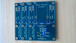
Did anyone use this PCB from Jim's?
How to mount the heatsinks for the MOSFETs is not entirely obvious.
Did anyone use this PCB from Jim's?
How to mount the heatsinks for the MOSFETs is not entirely obvious.
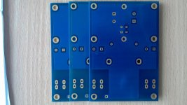
Interesting upgrade of the PCB. In this arrangement I think you have to mount the power MOSFETs directly on the case, and this is how Blowtorch was designed to address heat removal from the box, apparently.
So with this arrangement you can have a sealed enclosure. Nice 🙂
Cheers!
So with this arrangement you can have a sealed enclosure. Nice 🙂
Cheers!
Strange though the MOSFETs are not located at the PCB edges. It is some distance to the enclosure wall (I guess that was what you meant)?
I observe it is more than one year since last post here, but I will try anyway.
Did anyone use this PCB from Jim's?
How to mount the heatsinks for the MOSFETs is not entirely obvious.
Hi Rønningstad,
It is an interesting new layout as metallicus69 is pointing out! They would be mounted under the board and the hole should be big enough to pass a screw and plastic isolator washer. I would put the board flush against the surface where it will officially be, take a marker through the screw holes to mark the screw hole positions then drill and tap. You will then have to bend the legs of the transistors to the upright position to go back on the PCB. I would do one or two transistors at a time, solder, unscrew and then do the next ones.
Here's some examples

Don't install this on a 1-2mm thick aluminum, it will get too hot once biased.
Let me know how this new JC-80 performs!
Ciao!
Do
Last edited:
I see, it requires a very thick bottom plate - heat sink - to cool the MOSFETs against. Or alternatively largish heat sinks on the PCB underside.
I am not sure I like this approach, however Jim is almost sold out of the first version (with the heat sinks standing on the PCB component side).
Thanks.
Regds
Rolv-Karsten
I am not sure I like this approach, however Jim is almost sold out of the first version (with the heat sinks standing on the PCB component side).
Thanks.
Regds
Rolv-Karsten
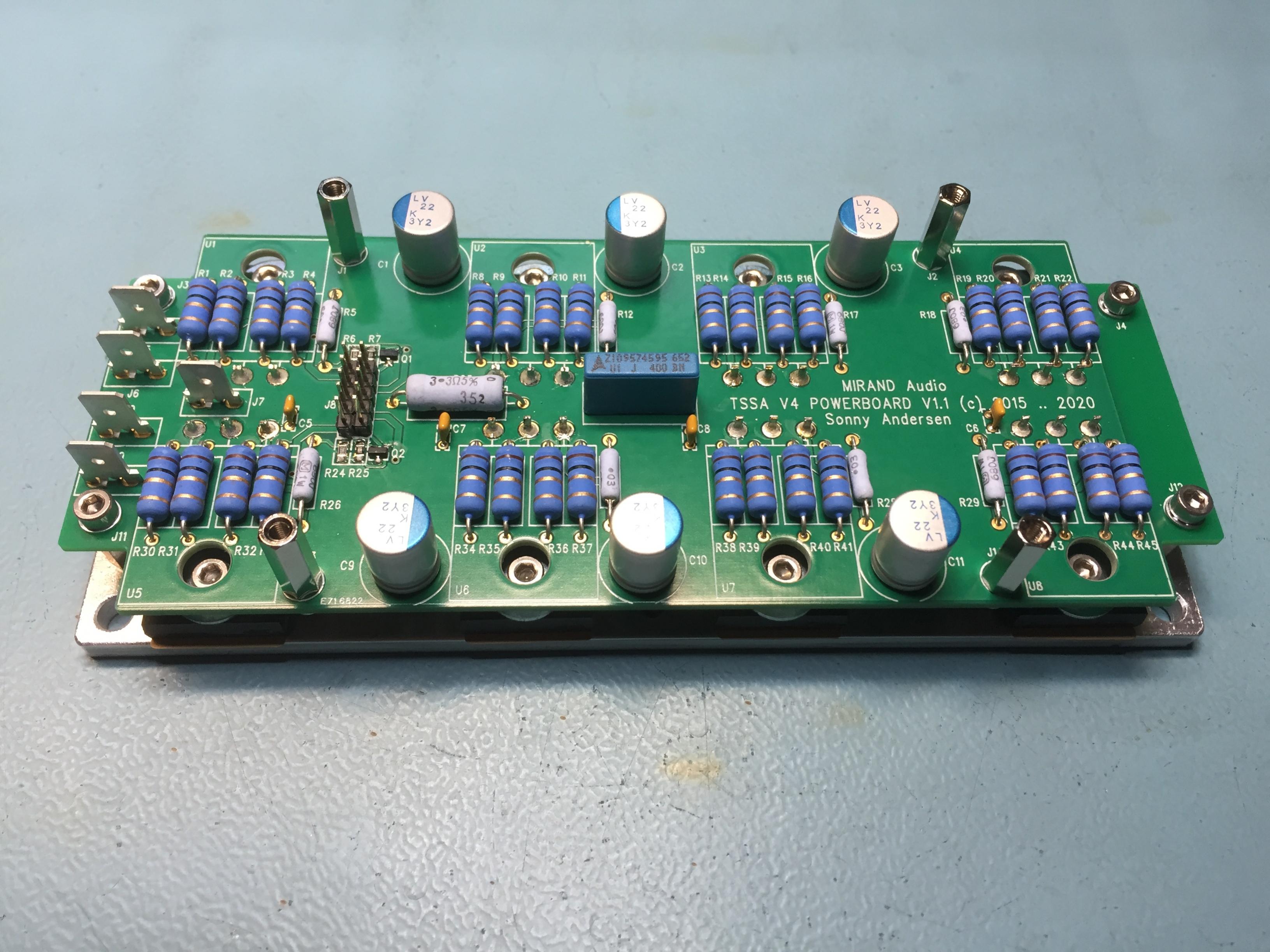
when the screw is tightened the transistor tends to turn and strains the leadouts and solder joints.
It is extremely difficult due to the transistor being under the PCB to hold it and prevent this turning as you tighten down.
Instead if you place a thin, maybe 1mm washer plate across all 4 devices and insert temporary screws in the open holes, then tighten the screw down on the installed devices. You get a straight down clamping action and the washer plate acts as the washer shown in the pic.
I have ordered a set from Jim and have already some matched lsk170/lsj74 with Idss around 22mA so I am ready to experiment a complementary differential folded cascode with this PCB (should be only minor mods). Only if I would have enough time on my hands 🙁
I also have a set of transistors from many years ago. Hitachi MOSFETs I have , i have to read me up on that with regard to what to use in the JC80.
the maximum Idss for a V grade k170/j74 is 20mA.I have ordered a set from Jim and have already some matched lsk170/lsj74 with Idss around 22mA..................
22mA devices must be fakes.
A, B & C grade are the equivalents to the Toshiba gr, bl & v grades.
Some time recently Linear introduced the D grade to the range.
If his "matched Idss" are the new Dgrade then they are likely to not be fakes.
If you look back at my testing you will see what I referred to as C+ grade because then Linear did not have a D grade. They stopped at C the equivalent to the 12mA to 20mA V grade from Toshiba.
- Home
- Source & Line
- Analog Line Level
- JC-80 eBay PCBs & Power Train