Wavebourn,
If this is so then what is the point of running the VAS at 1A idle, if a triple or quad EF stage at output cannot get away with reflection.
Except reflections Kirk and Early effects exist. The more of EFs you add, the less linear they are.
Happiness is not about quantity, but about quality.
EF and transformer may good idea. This mine, small, high current, also fast enough.
Right; I like bootstraps too, as I mentioned before.
CBS240,
any kind of feedback worsen the isolation between stages. The common collector amplifier provides poor isolation because of the high inherent feedback. The (varying) load has a great impact on linearity, but the distortion due to an added stage can be worse. What kind of error amplifier do you mean? The driving stage after the VAS should be a FET.
The distortion from the output stage, and with class AB there will be the load dependent distortion as well as high frequency content related to crossover, will translate to relative changing impedance that the VAS must cope with. Using FETs for drivers does not necessarily mean the VAS will not see a varying Z. The high frequency terms of crossover will require varying current from the VAS to drive the gates of the FET drivers all the same. Class A significantly simplifies this issue, but comes at a stiff price. The trans-impedance amplifier does not like this changing load impedance. The output Z of the CB stage cannot be reliably controlled by the global loop, it must remain constant for best performance. The local error amplifier 'linearizes' the output stage thus providing a much more linear and constant impedance to the VAS, particularly regarding HF content.
I am referring to an error amplifier that measures the difference between the output of the VAS and the final output that drives the load, and uses both feedback and feedforward to generate an anti-distortion signal that is summed with the audio signal and fed to the output devices. The load Z this stage would provide to the VAS would be the same no matter the conduction state of the output devices. One example might be like Dr Hawksfords work with EC for Darlington outputs, or other variations of local error correction.
To design an amplifier with a nonlinear transfer function representing each stage and the coupling of multiple stages, then slapping a feedback loop around it in a futile attempt to 'correct' all the ills created by the nonlinearities is bad practice due to the limited bandwidth of the global loop. Your opinion may differ on this but each stage together should present as linear as possible of a function to the global loop. This may include local nested FB/FF networks to deal with particular types of distortion such as crossover and load dependent distortions. This is the beauty of the trans-impedance amplifier if it is driving a constant load Z, it provides a very linear transfered voltage to the global loop. Since the majority of distortion comes from the output stage, this is the big beast to tackle first. Adding an extra stage in return for linerizing the function within the global loop that it must deal with is a good trade off in terms of overall distortion, IMHO. 🙄
The best VAS is relative and depends on the circuit it is used in.
I am referring to an error amplifier that measures the difference between the output of the VAS and the final output that drives the load, and uses both feedback and feedforward to generate an anti-distortion signal that is summed with the audio signal and fed to the output devices.
Right;
and in my class A+C amp the entire class C output stage senses this difference and corrects it increasing emitter current as soon as the difference increases. 😉
Once again: resistor from VAS supplies load by current. Inputs of class C followers are connected to the left side of this resistor (to VAS output), outputs of that class C followers are connected to right side of the resistor (to the load). Voltage drop on the resistor is proportional to output current, so as soon as it's sufficient to be sensed by output class C followers, they start providing output current bootstrapping VAS output through still the same resistor. It happens on loudness far from zero volt threshold, so it is much less audible than in case of class AB transistor amp that spoils "first watt" introducing distortions during precious zero-crossing phase.
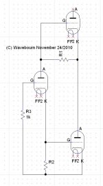
Here is another example of such bootstrap, but for different topology:
Attachments
Jan,
I'm finding myself being in an intersubjective agreement with your approach addressing the epistemological challenge to explain the metaphysical paradox of perceptual experience and physical fact.
😀
I'm finding myself being in an intersubjective agreement with your approach addressing the epistemological challenge to explain the metaphysical paradox of perceptual experience and physical fact.
😀
By the way,
why should we aim for consensus? Can someone genuinely agree with everything? Such discussions would not just be boring, but also genuinely false. Who would be the winner? The sycophant?
why should we aim for consensus? Can someone genuinely agree with everything? Such discussions would not just be boring, but also genuinely false. Who would be the winner? The sycophant?
Kanwar,
Likewise, the voltage gain of the common emitter amplifier, converting voltage-to-current, in a cascode is just about one (with a common base amplifier). The voltage gain of JFETs is more complicated to calculate.
The only purpose of impedance matching is to minimize losses, it does not ensure anything else, especially not low distortion, as mentioned earlier, efficiency and linearity don´t like each other. The lack of current gain enhances linearity, in a cascode the common base amplifier acts as a current buffer.In common base amplifier, the signal is injected into emitter which is low impedance node and it certainly requires a source with matched impedance, since there is no current gain in CB stage , you only have a voltage gain at collector.
Likewise, the voltage gain of the common emitter amplifier, converting voltage-to-current, in a cascode is just about one (with a common base amplifier). The voltage gain of JFETs is more complicated to calculate.
sumaudioguy,
you have made some correct observations as well.
you have made some correct observations as well.
Exactly, and during that time grave distortions occur...That "feedback" is all very nice for steady state but feedback takes time and during that time the load is bad. Every amp I have tested using these schemes illuminated above oscillates easily during the "waiting for the feedback to arrive" interval. Therefore, for audio it does not really work.
Jan,
I'm finding myself being in an intersubjective agreement with your approach addressing the epistemological challenge to explain the metaphysical paradox of perceptual experience and physical fact.
😀
Actually, I think this is your first post here that makes some sense...😉
jan didden
Kanwar,
The only purpose of impedance matching is to minimize losses, it does not ensure anything else, [snip].
This is incorrect. It should be immediately clear that to minimize losses you AVOID impedance matching. Minimum losses are when you match a low output impedance voltage source with a high-impedance load 🙄
jan didden
That "feedback" is all very nice for steady state but feedback takes time and during that time the load is bad. [snip].
This is NOT true. Feedback reacts immediately, continuously. There is no delay, except for a sub-usec through the amp. Any change in output voltage immediately leads to a change in feedback signal. You are confusing delay with phase shift which is something completely different.
Read my blog on feedback: How to be on time everytime etc.
http://www.diyaudio.com/forums/blogs/janneman/454-feedback-how-late-time-same-time-all-time.html
jan didden
The only purpose of impedance matching is to minimize losses,
if the "loss" he wishes to minimise is Power, then equal impedance for transmit and receive ends do achieve maximal power transfer.This is incorrect. It should be immediately clear that to minimize losses you AVOID impedance matching.
If the loss of voltage transfered is to be minimised then lowest RS and highest Rin do maximise the voltage at the receive end.
By janneman-except for a sub-usec through the amp.
But is that still not time ?? "Delay" is a gross expression of time, inappropriate for the ultrashort group delay of a closed loop design.
So.. after reading your blog , I see the myth "busted". Still ,time-(t) is a component in all the phase shift functions. Phase (waves) - Wikipedia, the free encyclopedia
I KNOW NFB works , it just has a harder time beyond the audio band (50khz+). 🙂
OS
Last edited:
Feedback is helpfull but may causing oscillation and very low output impedance, use it with care.
Most power loss in audio amplifiers are dissipated at linear transistors, here are interesting class A +PWM schematic showing up, it may similar version with class A+C with difference just between smooth for A+C and switch for PWM. Also using mosfet as VAS directly powering the load, and opamp feedback.
http://www.diyaudio.com/forums/solid-state/144726-switching-current-source-class-10.html#post2377043
Also, comparison of THD measurement I ever simulated class A, AB, and B operated at same amplifier, resulting that class A has lowest THD. Also effect of feedback used for error corrections and speed up effect. Hope it useful.
http://www.diyaudio.com/forums/ever...si-not-bad-really-i-post-some-proof-here.html
What amp built with discreet transistors has a propagation delay in the "sub microsecond" range? This amp right here is 4.3µS to go from plus input to output and is one of the faster amps tested. Almost all amps tested have been slower. With many using 30MHz output devices that microsecond is a long time to wait for feedback to happen. I think janneman is confused about propagation time in discreet power amps. This confusion leads many to build marginally stable (bad sounding) amplifiers which almost all of the amps tested here are. Over 99% are unstable being very easy to cause oscillation. By the way, I am extremely clear on how all this time stuff works with many saying I am the one of few that do. Phase shift can also be quantified as time delay. It matters not how it is called it is still delay and still a big problem if loop feedback is used. As for janneman's discussion of phase margin... this is deeply dependent on load and with power amplifier driving bad loads the phase margin can very quickly equal near zero. This is why it is so very important for the last voltage gain stage to be able to drive the reflected load from the output stage... so stability can be maintained.
Last edited:
4.3uS delay are very slow indeed for now GHz era. It may oscillated to reach 20KHz 50Vrms slewrate with only 30dB NFB. Better using low NFB and let it has light sound. High NFB causing high DF that are bad sounding. Using local feedback also could increase linearity and component speed by forcing it, then global feedback could be increased.
I am now using a Powergain, it gaining forward power by 100x and reducing reflected power by 0.01x. It need less than 200ns delay to work properly with the conditioning amplifer as input.
I am now using a Powergain, it gaining forward power by 100x and reducing reflected power by 0.01x. It need less than 200ns delay to work properly with the conditioning amplifer as input.
Last edited:
Most of the present amps simulated and built at DIYA that are absolutely stable in every way average about 100nS (1/10th uS - below) propagation delay input-output. 1 cycle of a 20KHZ waveform is 20uS !! At 4.3uS you might have a good bass amp , but be severely limited at the higher frequencies.
OS
OS
Attachments
I have the 1979 Siliconix VDMOS Fet Design Catalog in my hand
it shows Shaeffer's DA76-1 (revised 9/77) "The VDMOS Power FET Audio Ampfiler" with:
"...1 Hz to 800 KHz response" - with fr graph and scope shots of 100KHz sq wave response
for the “uncredentialed” who may not have the approximations memorized (or in my long out of school case just derive them from the engineering principles I do recall with decent math software) the response plot shows no peaking so the 1st order filter 1/(2*pi*800KHz) ~= 200 nS time constant aproximation is fine, so group delay ~= 200 nS for all audio frequencies
so 33 years ago it was already possible to build "sub microsecond delay" audio power amplifiers
(my credential is actually a Biology degree - but I discovered in my Junior year "24 hour lab" that I wasn't cut out for Science - all of my friends were EE/CS and the "instant feedback" from changing code or component value sure beat waiting for weeks to see if the spots growing in the grids on your petri dish may mean something - a few linear systems and control theory courses later and I "got" electronic design and have earned my living doing it ever since – with lots of continuing self-education along way)
Last edited:
"...1 Hz to 800 KHz response" - with fr graph and scope shots of 100KHz sq wave response
for the “uncredentialed” who may not have the approximations memorized (or in my long out of school case just derive them from the engineering principles I do recall with decent math software) the response plot shows no peaking so the 1st order filter 1/(2*pi*800KHz) ~= 200 nS time constant aproximation is fine, so group delay ~= 200 nS for all audio frequencies
so 33 years ago it was already possible to build "sub microsecond delay" audio power amplifiers
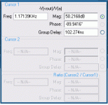
Few months ago I was playing with a schematics very similar to this one (it was with jFET-BJT composite transistor)
http://www.diyaudio.com/forums/atta...ressions-follower_99-bsp129-_fqaf44n08-ss.jpg
Its responce (10V p-t-p, 4 Ohms resistive load) was well above 3MHz, and delay estimated from sine signal shift at 1MHz was near 20ns.
- Home
- Amplifiers
- Solid State
- It's 2010 and what's your fav VAS transistor?