Glenn Kleinshmidt has shown through measurement and it can readily be seen in simulation that electrolytics can resonate badly with film bypass. This can cause circuits to become unstable as I have observed on my bench. Furthermore chipregs have significant output inductance which resonates at audio frequencies with electrolytics.
I could clearly observe ringings on the raw outputs of the SMPS at the switching frequency. If I remember correctly, it takes at least 6 or 7 cycles of possibly 30mV ptp for it to settle down. I wouldn't think Marantz would release a product with this quality. Take the 5V output as an example, the 2 x 16V 1500uF Panasonic FR has an impedance of 0.009R at 100kHz. I don't know if there is any chance that the secondary leakage inductance of the RF transformer, the diodes and the Panasonic FR form a LCR tuned circuit, worsen by the fact that the cap impedance being low. Of course, I am only speculating.
Perhaps all SMPS outputs are as dirty as that. Since I have not worked with SMPS so I really don't know if that is normal or not. No matter how stiff I can come up with filters, I wouldn't feel good if the PSU is ringing.
I found that the midrange sound quality was degraded a bit from the original player. This may well be due to the rings I introduced, or perhaps that it was there in the original player but at that time was heavily masked by the RF noise, and once I have (now) got rid of the RF noise it unmasks it? I would not know.
I guess the plan of attack would be to do more thorough measurements and damp the ringings...
Having done a great deal of simulation in this area, I don't see this happening at all. Could you point to a specific link, or give a precise example, please?Glenn Kleinshmidt has shown through measurement and it can readily be seen in simulation that electrolytics can resonate badly with film bypass.
Here is Glenn's page:
Capacitors in parallel - real life measurements
There is an interesting bump at 30-40KHz that could be a instrument error or the mechanical resonance of the capacitor but Glenn decides not to say anything about it so we don't know.
And this is on chipregs:
Just one thing about music - when it hits you feel no pain
Thanks, I can see 2 effects here: one is that the ESL of the electro is starting to rise before the C of the bypass has a chance to kick in, so we are seeing the impedance behaviours of the two parts overlaid - this is not a resonance; and, he is allowing for a lot of layout parasitics to get into the action - if the layout is contributing major elements of the behaviour, then you're not actually doing bypassing correctly.
I'm not happy with his simulation, and the values inserted ... what I will do is recreate the circuit he posted, and determine precisely what are the critical areas. At these frequencies every little parasitic counts, and sometimes what seems to be meaningful is actually of little real significance ...
I'm not happy with his simulation, and the values inserted ... what I will do is recreate the circuit he posted, and determine precisely what are the critical areas. At these frequencies every little parasitic counts, and sometimes what seems to be meaningful is actually of little real significance ...
Resonance is always a capacitive impedance and an inductive impedance overlaid; what you don't see on the chart is the phase interaction which causes impedance to spike. The film bypass resonates with the ESL of the electrolytic in parallel resonance mode causing the impedance spike. Neither the bypass nor the lytic have enough ESR to damp this, which you know because for both components the impedance curve at the resonance frequency is primarily reactive, not resistive.
If you can show that the resonance can be eliminated without intentional snubbing, that will be very useful to know.
If you can show that the resonance can be eliminated without intentional snubbing, that will be very useful to know.
Thanks, I can see 2 effects here: one is that the ESL of the electro is starting to rise before the C of the bypass has a chance to kick in, so we are seeing the impedance behaviours of the two parts overlaid - this is not a resonance; and, he is allowing for a lot of layout parasitics to get into the action - if the layout is contributing major elements of the behaviour, then you're not actually doing bypassing correctly.
I'm not happy with his simulation, and the values inserted ... what I will do is recreate the circuit he posted, and determine precisely what are the critical areas. At these frequencies every little parasitic counts, and sometimes what seems to be meaningful is actually of little real significance ...
Frank, we've had this same disagreement, before. These LC resonances do happen. I have had them happen in SMPS's I have designed and built. It's a lot more obvious in those types of "non-audio' (signal-wise) circumstances, where you have fast edges trying to suddenly start and stop, or even just some leftover spikes to excite things. You can get horrendous ringing that can even be rail-to-rail, sometimes, and half a period long or more. Sometimes it even kills other components, within seconds.
The cure is usually a snubber resistor, often with a series capacitor, which, by the way, is only needed so that only the unwanted frequencies can "see" the resistor, so that the resistor's power rating can be lower and not as much energy is wasted.
For an already-built system, it's relatively easier to find the optimal snubbing resistance value. It's just the characteristic impedance of the LC circuit formed by the L and C in question. But there's an easy trick for finding that! You don't even have to mess with the L or the C. Just snub it and the HF should be completely gone.
The most-efficient way to do it requires a scope: (Or maybe just a frequency counter would work. And a spectrum analyzer would be better than either one.)
http://www.diyaudio.com/forums/powe...lm-caps-electrolytic-caps-30.html#post2828689
I had a linear supply, once that had bad rectifier diode switch-off ringing, at 14 MHz or so. The transformer was way oversized. I think that the parasitic capacitance turned out to be 20 pF or so (mostly from the diodes, I guess). I think the transformer's leakage inductance was high. Anyway, the optimal snubber resistance turned out to be something like 5 kOhms! So I didn't even really need a capacitor, although I used one anyway, so I could use a 1/4-Watt R. I didn't even believe it, at first. But I stuck it across the transformer secondary and VOILA, everything was clean as a whistle.
Last edited:
Tom, you've got me!! I've just run a few little simulations, which have focused on the higher end of the spectrum, and there they are! It was quite some years ago that I did the previous rounds of playing with this, and I suspect the number of intervening years, and the fact that I was concentrating on optimising in the 100k-10MHz area at the time caused me to overlook this, misconstrue the bigger picture.
So, my humble apologies for pushing this line, which is incorrect. However, the benefit is, for me, and hopefully others, that I will now do some major investigation into precisely what matters amd what doesn't, and come up with some rule of thumb guidelines which can nail it every time ...
Cheers,
So, my humble apologies for pushing this line, which is incorrect. However, the benefit is, for me, and hopefully others, that I will now do some major investigation into precisely what matters amd what doesn't, and come up with some rule of thumb guidelines which can nail it every time ...
Cheers,
And, now that I'm more strongly reminded of the results I was getting back then, I do recall never bothering playing with the values of film caps that can get you into trouble, because they are of almost zero benefit in improving the bypassing - unless I get something like an order of a magnitude improvement in some parameter, or performance behaviour I don't really see the point ...
looks like the links are still OK
I've looked into bypassing in ADC precision instrumentaiton applications - there are newer low inductance SMT "wide" termination caps and multi-terminal types for multi-MHz work - you're bascially screwed if you have to use through-hole parts
there is some info on what really happens in bypass applications and random paralleling of different caps can result in impedance peaks in the supply impedance
http://www.ultracad.com/articles/esrbcap.pdf shows the "anti-resonance" impedance peak you can get with the wrong choice of caps in parallel
http://www.pa.msu.edu/hep/d0/ftp/ru...nformation/xilinx_xapp623_decoupling_caps.pdf
also shows measured ps impedance peaking
the plots show ESR isn't always bad - lowers impecance peaking even if ultimate low Z is limited - sometimes introducing discrete R is a good idea
Thanks, jcx. The Ultracad document I had since 2004, the Xilinx nicely backs it back - demonstrating that if the need for very low impedance, at very high frequencies is an absolute must, then there is a way ...
I did some measurements again.
When the earth probe was connected to the chassis near the star ground point and the measuring probe was floating in the air around the area of the SMPS transformer, the wave forms were clearly seen.
Made no mistakes - there is 100kHz switching frequency. Imagine square waves are joined together. When rising to the top there is obvious ringing at a frequency between 10MHz and 100MHz. The ringing lasts until about half wave then settles down. Immediately following that there are a few larger amplitude waves extending until near the end of the square wave. Then when the wave goes down to the bottom, there is another similar ringing at a frequency between 10MHz and 100MHz. The waves look artistically "pretty".
Put the probe on the rails. All three rails look very similar. When zoomed out to 100mV/Div, 10us/Div, it looks like DC but with spikes (in a vertical line) at the switching frequency, typical of SMPS output, perhaps. When zoomed in, all the dirts are reviewed.
Obviously the switching spikes between 10MHz and 100MHz are passing through the passive LCR filters with little suppression.
The switching noises are up to 100mV peak to peak, not 40mV. That is noisy!
Measurements comparing the input to the output of my 2nd order LP filters with ferrite beads showed some small amount of suppression of 10MHz to 100MHz noise, but far short of the result shown in simulations.
But then I have to say that the ground point is fairly far away from the ground point near the measurement, as I have nothing to clip the earth probe on. I don't have RF probes. So I must not trust my measurements at these frequencies.
In terms of snubber, the Marantz has 3 secondary outputs of +12V, -12V and +5V. The +12V has a 1nF + 22R in parallel to the diode. The +5V has a 2n2 + 22R in parallel to the diode. There is no snubber to parallel the -12V diode.
So it appears that Marantz may have put in some efforts to damp the resonances.
Unfortunately, I have gone too far now and I won't replace all the low ESL caps with higher ESL caps in order to measure the differences. I do think that it is actually better to use low ESL/ESR caps and put in a 0.1R at the outputs of the diodes. But in reality, this requires cutting tracks and there may be space restrictions, something probably not feasible to do.
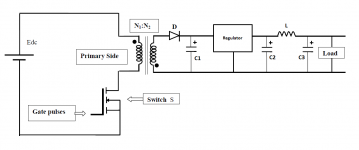
Referring to the simplified SMPS schematic attached, can we conclude that all major resonances come from Tx, D (i.e. Cd) and C1?
My 2nd order filters are in replacement of C2, L and C3 on the Marantz SMPS board.
So it appears that Marantz may have put in some efforts to damp the resonances.
Unfortunately, I have gone too far now and I won't replace all the low ESL caps with higher ESL caps in order to measure the differences. I do think that it is actually better to use low ESL/ESR caps and put in a 0.1R at the outputs of the diodes. But in reality, this requires cutting tracks and there may be space restrictions, something probably not feasible to do.
Referring to the simplified SMPS schematic attached, can we conclude that all major resonances come from Tx, D (i.e. Cd) and C1?
My 2nd order filters are in replacement of C2, L and C3 on the Marantz SMPS board.
Attachments
I never knew that this project is getting more and more complicated and interesting.
It seems that at these frequencies the ordinary chokes are not doing much. I have already selected shielded chokes with self resonant frequency of 58MHz but they may not live to their spec.
Perhaps what I need is more ferrite beads. Since the video quality is now degraded I think I should remove the 2nd order LP filter on the 12VM branch. This is the one that has the longest wires due to limited space so it may not be working as intended. Since the 2nd order LP filters were installed on the +/-12VA rails the treble harshness was further reduced so they could stay. Or perhaps they can be reversed back to 1st order LP filter with more ferrite beads in series, as measurements seem to suggest that the noise sits between 10MHz to 100MHz.
After that, the next thing I can try is to replace some of the lower quality diodes with fast and soft recovery type diodes and see if they reduce the switching noise. And last but not least, install some RC snubber from the transformer secondary to ground by observing the resonant frequency.
One thing you may try is to add series resistors to the small caps connected to the chassis. These are at much risk for ringing I think. The leakage capacitance of the trafo may be ringing, in which case you would want to measure it and try an RC snubber across the isolation gap (sacrilege!).
There is also the possibility of your inductors picking up SMPS noise and injecting it back into the supply. This could easily be tested by probing an inductor and holding it near the LCR filters to see what it picks up. The inductors of course are also radiating any signal that they block, so they may be radiating to inductors further down the LCR chain.
There is also the possibility of your inductors picking up SMPS noise and injecting it back into the supply. This could easily be tested by probing an inductor and holding it near the LCR filters to see what it picks up. The inductors of course are also radiating any signal that they block, so they may be radiating to inductors further down the LCR chain.
I have a computer smps open beside me.
I keep looking back at it hoping I will eventually work out what all the transformers (there are 3 off the HV) are doing.
But in the meantime I have roughly counted the numbers of R+C snubbers around the PCB. There are over a dozen.
Some body recognised how important it was to attenuate the ringing.
One thing you may try is to add series resistors to the small caps connected to the chassis. These are at much risk for ringing I think. The leakage capacitance of the trafo may be ringing, in which case you would want to measure it and try an RC snubber across the isolation gap (sacrilege!).
There is also the possibility of your inductors picking up SMPS noise and injecting it back into the supply. This could easily be tested by probing an inductor and holding it near the LCR filters to see what it picks up. The inductors of course are also radiating any signal that they block, so they may be radiating to inductors further down the LCR chain.
Good thoughts.
Where there is RF current, there is EMI radiation. Since at the frequency of switching spikes, a straight wire is an inductor so there is nowhere to escape from the RF emission. Perhaps some aluminium sheet partition / shield would work by the way of eddy current transferring RF current into heat. Your comment makes me think that the reason that my 2nd order LP filter does not work as well as intended may partly be due to circuit boards picking up emmitted RF.
As for caps connecting ground to other ground / chassis, they are on the primary side of the SMPS board, and on the digital ground of the DAC board. If we add series resistance to the caps we would degrade the caps' function, wouldn't we? I think the idea of the cap is to connect the ground to the other ground / chassis at higher frequencies but not DC. Adding resistance would disconnect in higher frequencies. Perhaps it may work if it is low ohm with a value just sufficient enough to damp any possible resonance. The trouble is that this would be almost impossible to measure.
This is something I have not thought through. I thought when connecting different grounds we would connect them in DC not AC because we only want a voltage reference, i.e. 0VDC aligned between grounds, and we don't want audio signal passing grounds and there shouldn't be currents running between grounds anyway. But the fact is that they do the opposite.
Try the snubber design procedure I posted, across the transformer secondary, for starters.
The usual case is that the leakage INDUCTANCE of the transformer makes an LC resonance with the capacitor that the diode becomes when it turns off. You would much rather stop the ringing right at its source, rather than trying to filter it somewhere downstream!
Putting a cap, alone, in parallel with a diode is just wrong! Always use the snubber design procedure I posted, instead! The RESISTOR is the snubbing element!! Without a resistor, there is nothing to dissipate the energy!
Depending on your probe, you might be able to devise a piece of thin, stiff wire to make a very short ground probe element. Often, the metal just behind and around the tip portion of the probe is the ground. A small piece of wire can go around it, and then out to the side for 1/8th to 1/4 inch, then bend to be parallel to probe tip and go down to same height. You won't be able to probe far-apart points (as you shouldn't).
Or, just buy a decent probe with the proper HF grounding and tip accessories.
OR, can you use two probes, in a differential mode?
ANOTHER approach is to simply install an RF connector, where you want to measure, and hook up some coax that goes to your scope input. But you would probably need a 50-Ohm or 75-Ohm scope input, or, an amplifier or matching circuit, or something. There is a schematic for a powered 1 GHz scope probe, in the thread at:
http://www.diyaudio.com/forums/equipment-tools/238615-hf-add-amplifier-my-oscilloscope-probes-4.html
The HF scope probe construction PDF is at:
http://elektrotanya.com/files/forum/2009/10/e04a036.pdf
Otherwise (or first, or also), try your probe-in-the-air trick, but get it CLOSE to different areas, and see if you can tell where the ringing is happening! Then find a way to probe across whatever is there, with the shortest-possible ground clip for the probe. Then try the optimal snubber design procedure!
WHY did you think that your filters should replace the C and L elements of the existing pi filter??!
You should be adding filters that are cascaded with that filter, if you hope to improve things significantly. Why not just add more LC stages to it, for example?
Remember that snubbers are quite small and could go on the bottom of the board. You could also put LC stages under there, to get short-enough leads etc. Maybe you would need some standoffs, for mounting the board, then.
If you are leaving ANY extra length of wire or leads, to make connections, it's not good.
For snubbers, we need to know the L and C. The cap across the diode has 1nF. The diode has 200pF. So it is 1.2nF.
The L comes from the leakage inductance of the transformer secondary winding. This is a tiny RF transformer. What leakage inductance do you expect? Would it give reasonable result by using an ordinary inductance metre (I have one) to measure it while shorting the primary? Would the reading be accurate enough?
Since we are dealing with 100MHz frequency, would non SMD snubber work? Bear in mind there is no way to get the non SMD snubber inductance below 20nH or something.
I imagine that I could install a 1k trimpot in series with a 0.022nF NPO, and turn the trimpot while observing the scope. But the inductance of the parts would possibly make the snubber not functioning.
- Status
- Not open for further replies.
- Home
- Amplifiers
- Power Supplies
- Is this real? - simulation of parasitics