Meanwhile, I found a source explaining why there was a BE resistor on the driver transistor. Adcom used this resistor in its older designs where there was a high supply voltage. This was significant due to the older transistors.You do need a series resistor in the base of the driver plus the cap.
View attachment 1394599
1. I don't understand what R301 and R401 are doing - these look like 68 Ohms? To be honest I've never used this and I haven't seen any other EF3 designs with these resistors.
2. The driver transistor emitter tie resistor R302 looks like 7.5 Ohms which means the driver emitter currents are 160 mA (c.f. 1.2V/7.5 ohms) which is extraordinarily high. In most EF3 designs, these are 33 to 68 Ohms and will still keep the driver in class A down to 2 Ohms at the full rail-to-rail output swing - you can always check this in LTspice as well.
3. For the pre-driver emitter tie resistor R314, you can safely set this at 120 to 150 Ohms - 750 Ohms is on the high side.
4. In some cases, a 10-33 ohm vase stopper in the pre-driver collector can also help.
5. Decoupling to the collectors of Q301 and Q402 looks good.
Many a great point and ots of great info here!
A bit more information:
1) Regarding Vce and Vcer (Vceo) ratings - today it's usually not a problem to find transistors that will withstand required voltages and tolerances between parts are not as high as in times past. A little background info - in most amplifiers the BE junction is bypassed by a resistor of some kind, the reason why this influences apparent breakdown voltage is becasue of C-B breakdown, which drives current into the base at high Vce and initially increases Ic, resulting in a formation of a 'knee' in the Vce-Ic curves at...

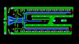
Hi, Dear Bonsai!I guess you are using a single-sided board, so having the supply rails and output rail adjacent to each other means you have minimized the overall loop areas and thus inductance which is good. If you use a double-sided board, you can lay them on top of each other for even lower inductance and loop area. I see you have brought your supply rails in on opposite sides of the board. I would suggest you bring the supply rails and associated 0V track next to each other in the middle of the board and run each rail alongside a thick ground track. That way you can provide a lot of bulk decoupling (220uF to 1000uF) plus HF decoupling (1uF X7R). Keep the supply rails close to the output rail as you have done as the supply rails and the output rail form a large high-power radiating loop that has to be minimized. The Zobel and output coil + damper resistor should be on this board as well in the middle.
How far away from the output board will you locate the input and VAS part of the amplifier?
Here is a snapshot of a board for some inspiration (its a double sided board)
View attachment 1395078
Is the following output PCB acceptable? Would it be worth making changes to it?