Oh, I see now, you're actually building one from scratch! Cool! Good project idea, I think the 565 is just a really elegant design. Walt Jung designed it BTW, though he didn't do the layout. Walt has probably written some things on output stage design that might shed light on why it is the way it is.
Huh, yeah the C4793 and NJW0281 ought to be close enough to the originals in fT and Cob... Though I am not aware of a confirmed working case. I know the MJE15032 with NJW0281 works though. Maybe try it just to see if it oscillates? I don't think this combo is the best, it's slower and the Cob on the 15033 is pretty high, due to its large silicon die and high power handling.
Huh, yeah the C4793 and NJW0281 ought to be close enough to the originals in fT and Cob... Though I am not aware of a confirmed working case. I know the MJE15032 with NJW0281 works though. Maybe try it just to see if it oscillates? I don't think this combo is the best, it's slower and the Cob on the 15033 is pretty high, due to its large silicon die and high power handling.
I should think with your nice compact layout for the output stage, that you might actually get away with less compensation. 🤔 The way the 565 (and many amps) is spread out like that is not a good thing. Big loops.
Do you separate power ground and signal ground?
It may cause issue if it is not implemented correctly. Try to short them together instead of separate them with 10 Ohm resistor.
Does it oscillate even without speaker connected?
It may cause issue if it is not implemented correctly. Try to short them together instead of separate them with 10 Ohm resistor.
Does it oscillate even without speaker connected?
jxdking:
The signal ground and the power ground are separated according to the original design. This should work well. The input is shorted. There is no load on the output.The circuit is currently set up according to the diagram: a traditional EF3 with a 10 Ohm driver base resistor. I compared it to a Quad 405 amplifier. In the photo, the Quad is on the bottom, and the GFA is on the top. The scope and probe errors are visible (?). I think this looks good.


You’re headed in the right direction 👍.I modified the circuit according to the diagram. It is now a typical EF3 layout. I removed the driver base resistor. I removed the pre-driver collector resistor. Currently, there is an initial 20 MHz oscillation with an amplitude of 100 mV. If there is a 10 Ohm resistor on the driver base, the oscillation disappears.
View attachment 1394919
I am out for a few hours but will come back later on. Do you have an output coil on this amp?
To test if this is an extraneous noise source, clip the scope ground to the scope tip. There should be no noise. Is the noise still there with the amplifier turned OFF?jxdking:
The signal ground and the power ground are separated according to the original design. This should work well. The input is shorted. There is no load on the output.
The circuit is currently set up according to the diagram: a traditional EF3 with a 10 Ohm driver base resistor. I compared it to a Quad 405 amplifier. In the photo, the Quad is on the bottom, and the GFA is on the top. The scope and probe errors are visible (?). I think this looks good.
View attachment 1394932View attachment 1394931
I see ripple even you shorted the input. Try to probe the ground make sure there is nothing on the signal ground at the first place. Your scope should be plugged into the same power strip/outlet that your amp uses. Oscilloscope ties its neg probe to the earth pin of the power cable by default. If your amp is not floating, you may introduce ground noise when probing.@jxdking:
The signal ground and the power ground are separated according to the original design. This should work well.
There is no coil on the output.
I connected the oscilloscope ground and the probe together. I connected this to the ground of the powered-off amplifier. Yes, the noise is still present this way.

I connected the oscilloscope ground and the probe together. I connected this to the ground of the powered-off amplifier. Yes, the noise is still present this way.
This is what my output board looks like. I wanted a simple design. Perhaps the NPN and PNP sections need to be better separated. I will redesign it into a simple EF3 layout.I should think with your nice compact layout for the output stage, that you might actually get away with less compensation. 🤔 The way the 565 (and many amps) is spread out like that is not a good thing. Big loops.

Unfortunately, that photograph of the assembled monobloc shows a suboptimal layout for all sorts of reasons and especially so for an EF3. I really don't know why they did that. The wiring inductances are going to be significant due to the large loop areas. With any output stage, incl. an EF2, you have to keep the OPS compact, the associated power, ground and output traces correctly grouped, and the tracks overlaid to keep the loop areas and associated inductances small. In the case of the Zobel network (absolutely mandatory with an EF3 using modern high fT devices), this has to be placed right at the output of the amp as close to the output devices as possible - which means within an inch. On the monobloc picture, it does not look like that is possible. I would question the lack of an output inductor on a feedback amp - that's quite a risky proposition IMV.I'll show a better picture. The NPN transistors are on the left side of the amplifier, and the PNP transistors are on the right side. (This is a monoblock.) There is a large distance between the boards. I just realized this. The driver also operated in Class AB. This way, only a few wires were needed between the boards. Now I understand why it’s not a classic EF3 layout.
In my amplifier, there will be only one output board.
View attachment 1394899View attachment 1394900
The good news is that noise then is not coming from your amplifier if you have turned it off. Sometimes this type of HF-conducted noise can come from networks that use the power line (I had one for a few years). The frequency looks like 5MHz so it is going to get in everywhere.There is no coil on the output.
I connected the oscilloscope ground and the probe together. I connected this to the ground of the powered-off amplifier. Yes, the noise is still present this way.
View attachment 1394934
Last edited:
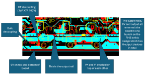
I guess you are using a single-sided board, so having the supply rails and output rail adjacent to each other means you have minimized the overall loop areas and thus inductance which is good. If you use a double-sided board, you can lay them on top of each other for even lower inductance and loop area. I see you have brought your supply rails in on opposite sides of the board. I would suggest you bring the supply rails and associated 0V track next to each other in the middle of the board and run each rail alongside a thick ground track. That way you can provide a lot of bulk decoupling (220uF to 1000uF) plus HF decoupling (1uF X7R). Keep the supply rails close to the output rail as you have done as the supply rails and the output rail form a large high-power radiating loop that has to be minimized. The Zobel and output coil + damper resistor should be on this board as well in the middle.
How far away from the output board will you locate the input and VAS part of the amplifier?
Here is a snapshot of a board for some inspiration (its a double sided board)

How far away from the output board will you locate the input and VAS part of the amplifier?
Here is a snapshot of a board for some inspiration (its a double sided board)
Attachments
Last edited:

I would still do some more work on this and include the other damping components normally associated with modern EF3 designs - i.e. driver base-collector capacitance, pre-driver collector decoupling etc. No point in rushing this only to find you have to go back and re-engineer it later.jxdking:
The signal ground and the power ground are separated according to the original design. This should work well. The input is shorted. There is no load on the output.
The circuit is currently set up according to the diagram: a traditional EF3 with a 10 Ohm driver base resistor. I compared it to a Quad 405 amplifier. In the photo, the Quad is on the bottom, and the GFA is on the top. The scope and probe errors are visible (?). I think this looks good.
View attachment 1394932View attachment 1394931
It’s interesting that the wiring in the picture works well in the original units. Perhaps because of the slower transistors.. In the middle of the picture, the brown and blue wires connect the pre-drivers to the VAS. In my amplifier, the driver wires are sensitive if they come close to other wires. I am using a single-sided PCB. Adcom didn’t use a coil on the output, not even in several older designs.Unfortunately, that photograph of the assembled monobloc shows a suboptimal layout for all sorts of reasons and especially so for an EF3. I really don't know why they did that. The wiring inductances are going to be significant due to the large loop areas. With any output stage, incl. an EF2, you have to keep the OPS compact, the associated power, ground and output traces correctly grouped, and the tracks overlaid to keep the loop areas and associated inductances small. In the case of the Zobel network (absolutely mandatory with an EF3 using modern high fT devices), this has to be placed right at the output of the amp as close to the output devices as possible - which means within an inch. On the monobloc picture, it does not look like that is possible. I would question the lack of an output inductor on a feedback amp - that's quite a risky proposition IMV.
The good news is that noise then is not coming from your amplifier if you have turned it off. Sometimes this type of HF-conducted noise can come from networks that use the power line (I had one for a few years). The frequency looks like 5MHz so it is going to get in everywhere.

I'd hate to drive a capacitive load without a coil. You should test with at least 1uF in // with your expected range of resistance load - I test with 1nF up to 2.2uF and 2 ohms and above. It's very easy to make an amplifier absolutely stable with any load if you use an output inductor. In the doc below, although it's a simple VFA, the principles regarding capacitive loading apply generally to any feedback amplifier. A lot of the older designs never used output inductors and relied on the speaker cable inductance which in many cases led to problems. Note, that the output L must always be in parallel with a 2.2 to 3.3 Ohm resistor - I did not show that in the doc below.
https://hifisonix.com/wp-content/uploads/2014/11/Output-L_1.pdf
You should be able to twist the V+, V- plus the driver signals and 0V together from the driver board to the output stage - again, it is all about keeping loop areas small and thus minimizing susceptibility to radiated signals (from the high current OPS) and mains noise pickup from the PSU and transformer.
Interesting. The output is currently a classic EF3. I removed the driver base resistors. There was oscillation, but it changed as I moved the output board. I noticed that moving the negative driver wire affected the oscillation. I replaced the wire, and now there is no oscillation. So far, I have used 4 types of wires to connect the VAS to the pre-driver base. The problem occurred with all of them. This is the best and simplest solution so far.

I was wrong. The solution is not good. I tried the other channel. It has the same layout, but the 20 MHz oscillation is present. I replaced the pre-drivers with MJE15032/15033 transistors. This eliminated the oscillation, but I see more noise. I will put the C4793/A1837 transistors back. I will use driver base resistors and capacitors.
This seems like a good document. What do you think?


This seems like a good document. What do you think?
I’ve seen that document before and it explains why EFs oscillate despite there being no voltage gain. The original solution I used in a power amp on 2007 came from a PSpice document discussing the same subject. In my case the OPS oscillated at 4-6 MHz. I was using slow 21193/4 OP devices, MJE1532/33 and BF471/2 pre drivers. I used 22 ohms and 1nf driver dampers, plus’s OP stage base stoppers and stoppers in the pre-drivers bases. It completely solved the problem. Bob Cordell covered this subject with an identical approach in his book in 2012. So this solution is out there and used widely as good practice. (Note this is an old design from nearly 20 yrs ago - I’ve learned a lot along the way 🙂 )
https://hifisonix.com/power-amplifiers/ovation-250/
Once you have the OPS stable, moving cables around etc should not affect stability at all.
https://hifisonix.com/power-amplifiers/ovation-250/
Once you have the OPS stable, moving cables around etc should not affect stability at all.
Last edited:
Thank you! Great read. I see you also used a 15 Ohm driver emitter resistor. (In the GFA585 circuit, there are also two series 7.5 Ohm resistors connected between the driver emitters.) I still don’t understand what negative effect the additional resistor on the driver base might have.
How can the appropriate resistor value be calculated? Is there a way to do this?
There are several topics about this on the forum, but no concrete answers.
How can the appropriate resistor value be calculated? Is there a way to do this?
There are several topics about this on the forum, but no concrete answers.
If you knew the Cib of the driver transistors, you could use T=RC to determine how long it takes to turn the driver off. Cib is not published. What is known, 30 ohm base resistor is 3 times the base resistor of 10 ohms. Shutoff time up to 3 times slower than before. The predriver transistor has to bleed the charge off the base junction of the driver down towards zero to shut off the driver transistor.I still don’t understand what negative effect the additional resistor on the driver base might have.
How can the appropriate resistor value be calculated? Is there a way to do this?
Slow turn off can lead to cross conduction of the output transistors. very bad. Only you with physical device and scope can observe whether cross conduction is there or not. Under all temperatures & input signals and loads. If you get cross conduction wrong, you get to buy up to 40 new output transistors. Plus your stage amp dies in the middle of a show somewhere, damaging your band's reputation.
One safe change is to make the 10 ohm driver base resistors inductive wirewound. Like the output resistor the speaker output coil is always wound around. See if that kills your oscillation when you move the predriver-driver wire around.
If not 6 turn inductors are all over the garbage piles of the developed world. Each dead PCAT supply has several. Each dead flat panel TV has more than that. Or make them with 6 turns wire around a AA battery. I know Peavey amps have a 800 uH output coil, and that is 14 turns #16 wire about that diameter. Put inductance series the driver bases, located as close as possible to the driver.
Or buy Self's book to determine what size capacitor goes where.
Last edited:
- Home
- Amplifiers
- Solid State
- Is this a case of noise or oscillation? How critical is the impact of this signal anomaly